SLAS955A March 2013 – July 2015 DRV10963
PRODUCTION DATA.
- 1 Features
- 2 Applications
- 3 Description
- 4 Revision History
- 5 Pin Configuration and Functions
- 6 Specifications
-
7 Detailed Description
- 7.1 Overview
- 7.2 Functional Block Diagram
- 7.3
Feature Description
- 7.3.1 Speed Input and Control
- 7.3.2 Spin up Settings
- 7.3.3 Motor Direction Change
- 7.3.4 Motor Frequency Feedback (FG)
- 7.3.5 Lock Detection
- 7.3.6 Soft Current Limit
- 7.3.7 Short Circuit Current Protection
- 7.3.8 Anti-Voltage Surge (AVS)
- 7.3.9 Control Advance Angle
- 7.3.10 Overtemperature Protection
- 7.3.11 Undervoltage Protection
- 7.3.12 OTP Configuration
- 7.4 Device Functional Modes
- 8 Application and Implementation
- 9 Power Supply Recommendations
- 10Layout
- 11Device and Documentation Support
- 12Mechanical, Packaging, and Orderable Information
Package Options
Mechanical Data (Package|Pins)
- DSN|10
Thermal pad, mechanical data (Package|Pins)
- DSN|10
Orderable Information
7 Detailed Description
7.1 Overview
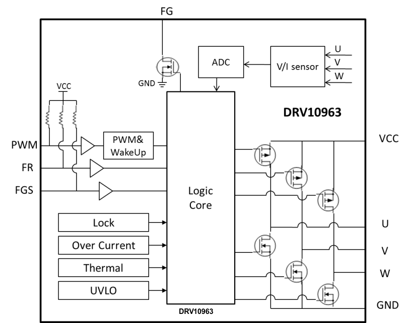
The DRV10963 device is a three phase sensor-less motor driver with integrated power MOSFETs. It is specifically designed for high efficiency, low noise and low external component count motor drive applications. The proprietary sensor-less window-less 180° sinusoidal control scheme provides ultra-quiet motor operation by keeping electrically induced torque ripple small.
Upon start-up, the DRV10963 device will spin the motor in the direction indicated by the FR input pin. The DRV10963 device will operate a three phase BLDC motor using a sinusoidal control scheme. The magnitude of the applied sinusoidal phase voltages is determined by the duty cycle of the PWM pin. As the motor spins, the DRV10963 device provides the speed information at the FG pin.
The DRV10963 device contains an intelligent lock detect function. In the case where the motor is stalled by an external force, the system will detect the lock condition and will take steps to protect itself as well as the motor. The operation of the lock detect circuit is described in detail in Lock Detection.
The DRV10963 device also contains several internal protection circuits such as overcurrent protection, overvoltage protection, undervoltage protection, and overtemperature protection.
7.2 Functional Block Diagram
7.3 Feature Description
7.3.1 Speed Input and Control
The DRV10963 provides 3-phase 25-kHz PWM outputs which have an average value of sinusoidal waveforms from phase to phase. When any phase is measured with reference to ground, the waveform observed will be a PWM encoded sinusoid coupled with 3rd order harmonics as shown in Figure 2. This encoding scheme simplifies the driver requirements because there will always be one phase output that is equal to zero.
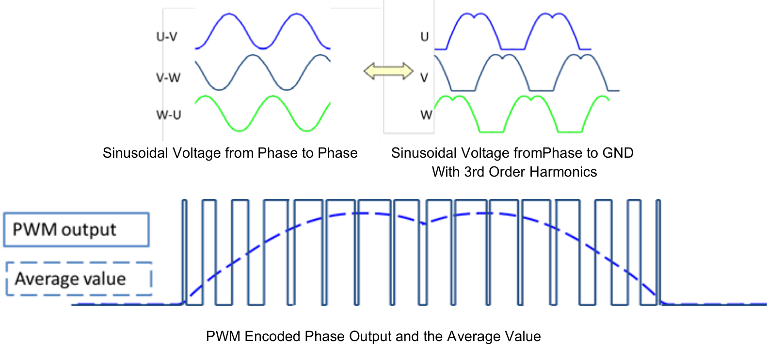 Figure 2. Sinusoidal Phase Encoding Used in DRV10963
The output amplitude is determined by the supply voltage (VCC) and the commanded PWM duty cycle (PWM) as described in Equation 1 and illustrated in Figure 3. The maximum amplitude is applied when the commanded PWM duty cycle is 100%.
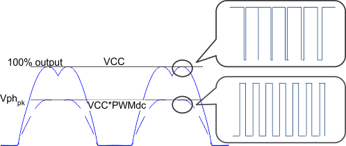 Figure 3. Output Voltage Amplitude Adjustment
The motor speed is controlled indirectly by using the PWM command to control the amplitude of the phase voltages which are applied to the motor.
The duty cycle of PWM input is converted into a 9 bit digital number (from 0 to 511). The control resolution is 1/512 ≈ 0.2%. The duty cycle analyzer implements a first order transfer function between the input duty cycle and the 9 bits digital number. This is illustrated in Figure 4, where τ=80 ms.
 Figure 4. PWM Command Input Controls the Output Peak Amplitude
 Figure 5. Example of PWM Command Input Controlling the Output
The transfer function between the PWM commanded duty cycle and the output peak amplitude is adjustable in the DRV10963 device. The output peak amplitude is described by Equation 1 when PWMcommand > minimum operation duty cycle. The minimum operation duty cycle can be set to either 13%, 10%, 5% or no limit by OTP setting (MINOP_DC[1:0]). Table 1 shows the optional settings for the minimum operation duty cycle. When the PWM commanded duty cycle is lower than minimum operation duty cycle and higher than 1.5%, the output will be controlled at the minimum operation duty cycle. When the input duty cycle is lower than 1.5%, the DRV10963 device will not drive the output, and enters the standby mode. This is illustrated in Figure 6.
Table 1. Minimum Operation Duty Cycle
| MINOP_DC[1:0] | MINIMUM OPERATION DUTY CYCLE |
|---|---|
| 0 | 0 (no limit) |
| 1 | 5% |
| 2 | 10% |
| 3 | 13% |
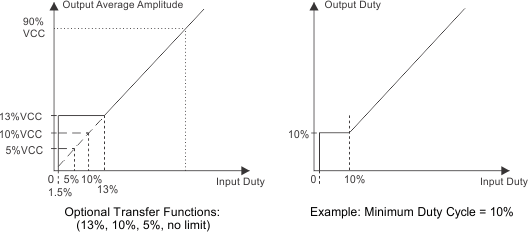 Figure 6. Speed Control Transfer Function
7.3.2 Spin up Settings
DRV10963 starts the motor using a procedure which is illustrated in Figure 7.
The motor start profile includes device configurable options for open loop to close loop transition threshold (HOffth), align time (TAlign), and accelerate rate (RAcc).
To align the rotor to the commutation logic the DRV10963 applies an x% duty cycle on phases V and W while holding phase U at GND. This condition is maintained for TAlign seconds. The x% value is determined by the VCC voltage (as shown in Table 2) to maintain sufficient driving torque over a wide range of supply voltages.
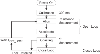 Figure 7. DRV10963 Initialization and Motor Start-up Sequence
Table 2. Align and Open Loop Duty Cycle
| VCC VOLTAGE | DUTY CYCLE DURING ALIGN AND OPEN LOOP (X)% |
|---|---|
| 5.25 to approximately 6 V | 43% |
| 4.5 to approximately 5.25 V | 50% |
| 3.75 to approximately 4.5 V | 60% |
| 3 to approximately 3.75 V | 75% |
| <3 | 100% |
When the align phase completes, the motor is accelerated by applying sinusoidal phase voltages with peak magnitudes as illustrated in Table 2 and stepping through the commutation sequence at an increasing rate described by RAcc until the rate of commutation reaches HOffth Hz. When this threshold is reached, the DRV10963 switches to closed loop mode where the commutation drive sequence is determined by the internal control algorithm and the applied voltage is determined by the PWM commanded duty cycle input. The open loop to close loop transition threshold (HOffth), align time (TAlign), and the accelerate rate (RAcc) are device configurable through OTP settings (HO_TH[3:0], TARA_TH[3:0]).
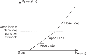 Figure 8. DRV10963 Start-up Profile
The selection of handoff threshold (HOffth) can be determined by experimental testing. The goal is to choose a handoff threshold that is as low as possible and allows the motor to smoothly and reliably transition between the open loop acceleration and the closed loop acceleration. Normally higher speed motors (maximum speed) require a higher handoff threshold because higher speed motors have lower Kt and as a result lower BEMF. Table 3 shows the configurable settings for the handoff threshold. Maximum speed in electrical Hz are shown as a guide to assist in identifying the appropriate handoff speed for a particular application.
Table 3. Motor Handoff Speed Threshold Options
| MAXIMUM SPEED (Hz) | HOffth (Hz) | HO_TH [3:0] |
|---|---|---|
| <100 | 12.5 | 1 |
| 100 to approximately 150 | 25 | 2 |
| 150 to approximately 200 | 37.5 | 3 |
| 200 to approximately 250 | 50 | 4 |
| 250 to approximately 300 | 62.5 | 5 |
| 300 to approximately 350 | 75 | 6 |
| 350 to approximately 400 | 87.5 | 7 |
| 400 to approximately 450 | 100 | 8 |
| 450 to approximately 500 | 112.5 | 9 |
| 500 to approximately 560 | 125 | A |
| 560 to approximately 620 | 137.5 | B |
| 620 to approximately 700 | 150 | C |
| 700 to approximately 800 | 162.5 | D |
| 800 to approximately 900 | 175 | E |
| >900 | 187.5 | F |
The selection of align time (TAlign) and accelerate rate (RAcc) can also be determined by experimental testing. Motors with higher inertia typically require a longer align time and slower accelerate rate while motors with low inertia typically require a shorter align time and a faster accelerate rate. System tradeoffs should be done to optimize start up reliability versus spin up time. TI recommends starting with choosing the less aggressive settings (slow RAcc and large TAlign) to sacrifice the spin up time in favor of highest success rate. Once the system is verified to work reliably the more aggressive settings (higher RAcc and smaller TAlign) can be used to decrease the spin up time while carefully monitoring the success rate.
Table 4 shows the configurable settings for TAlign and RAcc.
Table 4. Motor Alignment and Accelerate Options
| TAlign (ms) | RAcc (Hz/s) | TARA_TH[3:0] |
|---|---|---|
| 40 | 150 | 1 |
| 80 | 140 | 2 |
| 120 | 130 | 3 |
| 160 | 120 | 4 |
| 200 | 110 | 5 |
| 240 | 100 | 6 |
| 280 | 90 | 7 |
| 320 | 80 | 8 |
| 360 | 70 | 9 |
| 400 | 60 | A |
| 440 | 50 | B |
| 480 | 40 | C |
| 520 | 30 | D |
| 560 | 20 | E |
| 600 | 10 | F |
7.3.3 Motor Direction Change
The DRV10963 can be easily configured to drive the motor in either direction by setting the input on the FR (Forward Reverse) pin to a logic 1 or logic 0 state. The direction of commutation as described by the commutation sequence is illustrated in Table 5.
Table 5. Motor Direction Phase Sequencing
| FR = 10 | FR = 01 | |
|---|---|---|
| Motor direction | U->V->W | U->W->V |
7.3.4 Motor Frequency Feedback (FG)
During operation of the DRV10963 device, the FG pin provides an indication of the speed of the motor. The output provided on this pin can be configured by use of an OTP setting (FGOPT) and by applying a logic signal to the FGS pin. The configuration of this output is defined in Table 6.
Table 6. FG Motor Status Speed Indicator Configuration
| MOTOR CONDITION | (FGS = 1) | FGOPT=1,(FGS = 0) | FGOPT=0,(FGS = 0) |
|---|---|---|---|
| DRV10963xxDSNR Normal Operation | Toggles once per electrical cycle | Toggles once every 2 electrical cycles | Toggles once every 3 electrical cycles |
As seen in Table 6, the FG pin can be configured to toggle either once per electrical cycle, once per 2 electrical cycles or once per every 3 electrical cycles. Using this information and the number of pole pairs in the motor, the mechanical speed of the motor can be determined.
The formula to determine the speed of the motor is:
or
The FG pin has built in short circuit protection, which limits the current in the event that the pin is shorted to VCC. The current will be limited to ISC_FG.
7.3.5 Lock Detection
When the motor is locked by some external condition the DRV10963 will detect the lock condition and will take action to protect the motor and the device. The lock condition must be properly detected whether it occurs as a result of a slowly increasing load or a sudden shock.
The DRV10963 reacts to lock conditions by stopping the motor drive. To stop driving the motor the phase outputs are placed into a high impedance state. To prevent the current which is flowing in the motor from being returned to the power supply (VCC) the DRV10963 uses an ANTI VOLTAGE SURGE feature. This feature is described in a following section. After successfully transitioning into a high impedance state as the result of a lock condition the DRV10963 will attempt to restart the motor after TOFF_LOCK seconds.
The DRV10963 has a comprehensive lock detect function which includes 5 different lock detect schemes. Each of these schemes detects a particular condition of lock as illustrated in Figure 9.
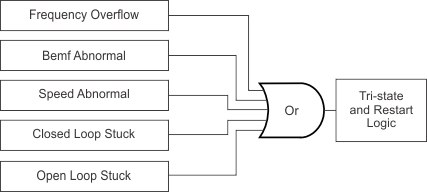 Figure 9. Lock Detect
The behavior of each lock detect scheme is described in the following sections.
7.3.5.1 Lock1: Frequency Overflow
For most applications the maximum electrical frequency of the motor will be less than 3 kHz. If the motor is stopped then the BEMF voltage will be zero. Under this condition, when the DRV10963 device is in the closed loop mode, the sensor less control algorithm will continue to accelerate the electrical commutation rate even though the motor is not spinning. A lock condition is triggered if the electrical frequency exceeds 3 kHz.
7.3.5.2 Lock2: BEMF Abnormal
For any specific motor, the integrated value of BEMF during half of an electronic cycle will be a constant as illustrated by the shaded green area in Figure 10. This is true regardless of whether the motor runs fast or slow. The DRV10963 monitors this value and uses it as a criterion to determine if the motor is in a lock condition.
The DRV10963 uses the integrated BEMF to determine the Kt value of the motor during the initial motor start. Based on this measurement a range of acceptable Kt values is established. This range is referred to as Kt_low and Kt_high. During closed loop motor operation the Ktc value is continuously updated. If the calculated Ktc goes beyond the acceptable range a lock condition is triggered. This is illustrated in Figure 11.
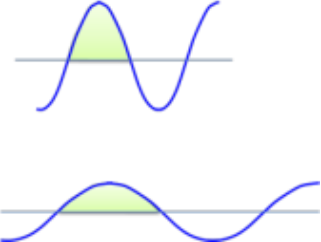 Figure 10. BEMF Integration
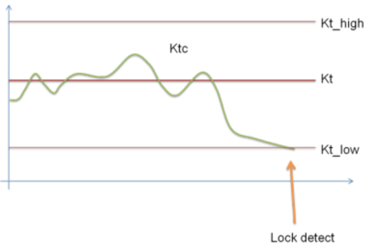 Figure 11. Abnormal Kt Lock Detect
7.3.5.3 Lock3: Speed Abnormal
If the motor is in normal operation the motor BEMF will always be less than the voltage applied to the phase. The DRV10963 sensorless control algorithm is continuously updating the value of the motor BEMF based on the speed of the motor and the motor Kt as shown in Figure 12. If the calculated value for motor BEMF is higher than the applied voltage (U) for a certain period of time (TON_LOCK) then there is an error in the system. The calculated value for motor BEMF is wrong or the motor is out of phase with the commutation logic. When this condition is detected a lock detect is triggered.
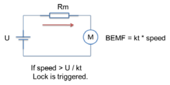 Figure 12. BEMF Monitoring
7.3.5.4 Open Loop Stuck
This lock condition is active when the DRV10963 device is operating in the open loop mode. When the open loop commutation rate becomes higher than the open to closed loop threshold (HOffth - see Figure 8) and the zero cross is not detected for the time corresponding to 2 electrical cycles then this is an indication that the motor is not moving. Under this condition the open loop stuck lock condition will be triggered.
7.3.6 Soft Current Limit
The current limit function provides active protection for preventing damage as a result of high current. The soft current limit does not use direct current measurement for protection, but rather, uses the measured motor resistance (Rm) and motor velocity constant (Kt) to limit the voltage applied to the phase (U) such that the current does not exceed the limit value (ILIMIT). This is illustrated in Figure 13 based on the calculation shown in Equation 5.
The soft limit is only active when in normal closed loop mode and does not result in a fault condition nor does it result in the motor being stopped. The soft current limit is typically useful for limiting the current that results from heavy loading during motor acceleration.
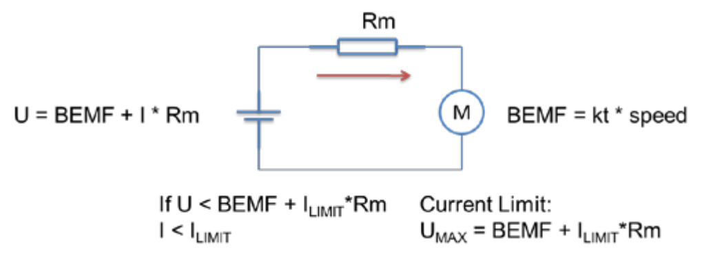 Figure 13. Current Limit
ILIMIT is configured by OTP setting (ILIMIT [2:0]) according to Table 7.
NOTE
The soft current limit calculation is not correct if the motor is out of phase with the commutation control logic (locked rotor). The soft current limit will not be effective under this condition.
Table 7. ILIMIT Settings
| ILIMIT [2:0] | ILIMIT |
|---|---|
| 0 | No current limit |
| 1 | 125 mA |
| 2 | 250 mA |
| 3 | 375 mA |
| 4 | 500 mA |
| 5 | 625 mA |
| 6 | 750 mA |
| 7 | 875 mA |
7.3.7 Short Circuit Current Protection
The short circuit current protection function shuts off drive to the motor by placing the motor phases into a high impedance state if the current in any motor phase exceeds the short circuit protection limit ISHT. The DRV10963 device will go through the initialization sequence and will attempt to restart the motor after the short circuit condition is removed. This function is intended to protect the device and the motor from catastrophic failure when subjected to a short circuit condition.
7.3.8 Anti-Voltage Surge (AVS)
Under normal operation the DRV10963 acts to transfer energy from the power supply to the motor to generate torque, which results in angular rotation of the motor. Under certain conditions, however, energy which is stored in the motor in the form of inductive energy or angular momentum (mechanical energy) can be returned to the power supply. This can happen whenever the output voltage is quickly interrupted or whenever the voltage applied to the motor becomes less than the BEMF voltage generated by the motor. The energy which is returned to the supply can cause the supply voltage to increase. This condition is referred to as voltage surge.
The DRV10963 includes an anti-voltage-surge (AVS) feature which prevents energy from being transferred from the motor to the power supply. This feature helps to protect the DRV10963 as well as any other components that are connected to the power supply (VCC).
7.3.8.1 Protecting Against the Return of Mechanical Energy
Mechanical energy is typically returned to the power supply when the speed command is abruptly decreased. If the voltage applied to the phase becomes less than the BEMF voltage then the motor will work as a generator and current will flow from the motor back to VCC. This is illustrated in Figure 14. To prevent this from happening, the DRV10963 buffers the speed command value and limits the rate at which it is able to change. The AVS function acts to ensure that the effective output amplitude (U) is maintained to be larger than the BEMF voltage. This prevents current from becoming less than zero. The value of BEMF used to perform this function is calculated by the motor Kt and the motor speed.
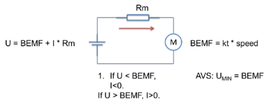 Figure 14. Mechanical AVS
7.3.8.2 Protecting Against the Return of Inductive Energy
When the DRV10963 suddenly stops driving the motor, the current which is flowing in the motor’s inductance will continue to flow. It flows through the intrinsic body diodes in the mosfets and charges VCC. An example of this behavior is illustrated by the two pictures in the top half of Figure 15. When the driver is active, the current flows from S1 to the motor and then to S6 and is returned to ground. When the driver is placed into a high impedance (tri-state) mode, the current goes flows from ground through the body diode of S2 to the motor and then through the body diode of S5 to VCC. The current will continue to flow through the motor’s inductance in this direction until the inductive energy is dissipated.
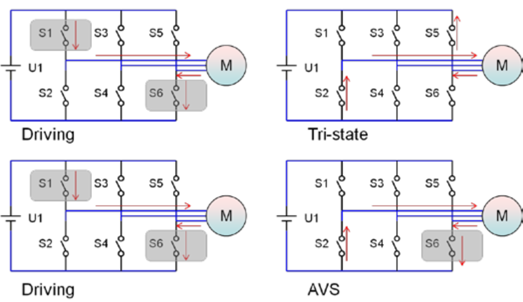 Figure 15. Inductive AVS
The lower two pictures in Figure 14 illustrate how the AVS circuit in the DRV10963 device prevents this energy from being returned to the supply. When the AVS condition is detected the DRV10963 device will act to turn on the low side device designated as S6. This allows the current flowing in the motor inductance to be returned to ground instead of being directed to the VCC supply voltage.
7.3.9 Control Advance Angle
To achieve the best efficiency it is often desirable to control the drive state of the motor so that the motor’s phase current is aligned with the motor’s BEMF voltage.
To align the motor’s phase current with the motor’s BEMF voltage the inductive effect of the motor must be considered. The voltage applied to the motor should be applied in advance of the motor’s BEMF voltage. This is illustrated in Figure 16. The DRV10963 provides configuration bits (CTRL_ANG[4:0] )for controlling the time (Tadv) between the driving voltage and BEMF. For motors with salient pole structures, aligning the motor BEMF voltage with the motor current may not achieve the best efficiency. In these applications the timing advance should be adjusted accordingly. This can be accomplished by operating the system at constant speed and load conditions and by adjusting the Tadv until the minimum current is achieved.
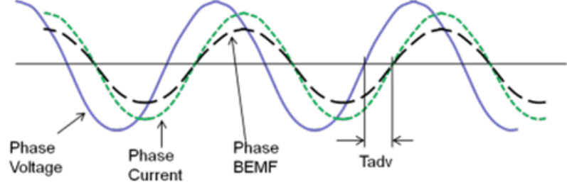 Figure 16. DRV10963 Advance Angle Control
Table 8. Control Advance Angle Settings
| CTRL_ANG[4:0] | Tadv |
|---|---|
| 0 | 0 |
| 1 | 20 µs |
| 2 | 40 µs |
| 3 | 60 µs |
| n | n × 20 µs |
| 6 | 120 µs |
| 8 | 160 µs |
| 31 | 620 µs |
7.3.10 Overtemperature Protection
The DRV10963 contains a thermal shut down function which disables motor operation when the device junction temperature has exceeded TSD. Motor operation will resume when the junction temperature becomes lower than TSD - TSD_HYS.
7.3.11 Undervoltage Protection
The DRV10963 contains an undervoltage lockout feature, which prevents motor operation whenever the supply voltage (VCC) becomes too low. Upon power up, the DRV10963 will operate once VCC rises above VUVLO_H. The DRV10963 will continue to operate until VCC falls below VUVLO_L.
7.3.12 OTP Configuration
The DRV10963 features OTP (one time programmable) bits to allow for flexible configuration of the device in order for optimization over a wide range of applications. Selection of various OTP options is described throughout this specification. The DRV10963JJ, DRV10963JM, DRV10963JU, and DRV10963JA parts listed in Table 10 are configured at the factory based on popular OTP settings for several different applications. TI provides EVM hardware along with a special GUI and a Motor System Tuning Guide which provides detailed instructions for determining the right part for your application. If your application requires settings not provided in any of the DRV10963Jx parts then the DRV10963P part can be used. The DRV10963P part provides blank OTP settings that can be configured for optimal performance in your application. The TI provided EVM and GUI will allow you to configure the OTP settings. Consult your TI representative if your application requires settings that are not available in the DRV10963Jx configurations described and if you are unable to use the DRV10963P option. The OTP bits used to configure the various part revisions are shown for reference in Table 10.
Table 9. OTP Configuration Bits
| OTP BIT NAMES | DESCRIPTION | REFERENCE TO |
|---|---|---|
| MINOP_DC[1:0] | Minimum operational duty cycle | Figure 6 |
| SLEEP_EN | Sleep mode enable | Standby Mode and Sleep Mode |
| TARA_TH[3:0] | Start-up time and accelerate setting | Spin up Settings |
| HO_TH[3:0] | Openloop to closed loop threshold. | Spin up Settings |
| ILIMIT[2:0] | Current limit setting. | Table 7 |
| CTRL_ANG[4:0] | Control advance angle. | Table 8 |
| FGOPT | FG output option. | Motor Frequency Feedback (FG) |
Table 10. The OTP Setting of the Factory Configured Parts
| MINOP_DC [1:0] | SLEEP_EN | TARA_TH [3:0] | HO_TH [3:0] | ILIMIT [2:0] | CTRL_ANG [4:0] | FGOPT | |
|---|---|---|---|---|---|---|---|
| DRV10963JJ | 2 | 1 | 7 | 8 | 4 | 6 | 0 |
| DRV10963JM | 2 | 1 | E | 4 | 4 | 6 | 1 |
| DRV10963JU | 2 | 1 | C | 7 | 4 | 6 | 0 |
| DRV10963JA | 2 | 1 | 7 | 8 | 4 | 8 | 0 |
| DRV10963P | 0 | 0 | 0 | 0 | 0 | 0 | 0 |
7.4 Device Functional Modes
7.4.1 Standby Mode and Sleep Mode
When the PWM commanded duty cycle input is lower than 1.5%, the phase outputs will be put into a high impedance state. The device will stop driving the motor. The device logic is still active during standby mode and the DRV10963 device will consume current as specified by IVCC.
When the PWM commanded duty cycle input is driven to 0% (less than VIL_PWM for at least TSLEEP time), the DRV10963 device will enter a low power sleep mode. In sleep mode, most of the circuitry in the device will be disabled to minimize the system current. The current consumption in this state is specified by IVCC_SLEEP.
The device will remain in sleep mode until either the PWM commanded duty cycle input is driven to a logic high (higher than VIH_PWM) or the PWM input pin is allowed to float. If the input is allowed to float an internal pullup resistor will raise the voltage to a logic high level.
Recovering from sleep mode is treated the same as power on condition as illustrated in Figure 7.
As part of the device initialization the motor resistance value and the motor Kt value are measured during the initial motor spin up as shown in Figure 7. Whenever the part is executing the initialization sequence it is important to note that the values determined by any previous spin up cycles no longer exist. In order for the motor resistance value and the motor Kt value to be properly initialized the system should be allowed to come to a complete stop before the next restart attempt.
Sleep mode can be disabled by OTP setting (SLEEP_EN). In this condition, the motor resistance value and the motor Kt value are preserved and the motor can reliably spin up without coming to a complete stop. This feature is referred to as the ‘re-synchronize’ function. If the ‘re-synchronize’ function is required the sleep mode cannot be used.