SLAS955A March 2013 – July 2015 DRV10963
PRODUCTION DATA.
- 1 Features
- 2 Applications
- 3 Description
- 4 Revision History
- 5 Pin Configuration and Functions
- 6 Specifications
-
7 Detailed Description
- 7.1 Overview
- 7.2 Functional Block Diagram
- 7.3
Feature Description
- 7.3.1 Speed Input and Control
- 7.3.2 Spin up Settings
- 7.3.3 Motor Direction Change
- 7.3.4 Motor Frequency Feedback (FG)
- 7.3.5 Lock Detection
- 7.3.6 Soft Current Limit
- 7.3.7 Short Circuit Current Protection
- 7.3.8 Anti-Voltage Surge (AVS)
- 7.3.9 Control Advance Angle
- 7.3.10 Overtemperature Protection
- 7.3.11 Undervoltage Protection
- 7.3.12 OTP Configuration
- 7.4 Device Functional Modes
- 8 Application and Implementation
- 9 Power Supply Recommendations
- 10Layout
- 11Device and Documentation Support
- 12Mechanical, Packaging, and Orderable Information
Package Options
Mechanical Data (Package|Pins)
- DSN|10
Thermal pad, mechanical data (Package|Pins)
- DSN|10
Orderable Information
10 Layout
10.1 Layout Guidelines
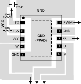
The package uses an exposed pad to remove heat from the device. For proper operation, this pad must be thermally connected to copper on the PCB to dissipate heat. On a multi-layer PCB with a ground plane, this can be accomplished by adding a number of vias to connect the thermal pad to the ground plane. On PCBs without internal planes, copper area can be added on either side of the PCB to dissipate heat. If the copper area is on the opposite side of the PCB from the device, thermal vias are used to transfer the heat between top and bottom layers.
For details about how to design the PCB, refer to TI application report, PowerPAD™ Thermally Enhanced Package (SLMA002), and TI application brief, PowerPAD™ Made Easy (SLMA004), available at www.ti.com. In general, the more copper area that can be provided, the more power can be dissipated.
10.2 Layout Example
 Figure 22. DRV10963 Layout Example