SLVSE89C August   2017  – June 2020 DRV10987

PRODUCTION DATA.  

  1. Features
  2. Applications
  3. Description
    1.     Application Schematic
  4. Revision History
  5. Description (Continued)
  6. Pin Configuration and Functions
    1.     Pin Functions
  7. Specifications
    1. 7.1 Absolute Maximum Ratings
    2. 7.2 ESD Ratings
    3. 7.3 Recommended Operating Conditions
    4. 7.4 Thermal Information
    5. 7.5 Electrical Characteristics
    6. 7.6 Typical Characteristics
  8. Detailed Description
    1. 8.1 Overview
    2. 8.2 Functional Block Diagram
    3. 8.3 Feature Description
      1. 8.3.1 Regulators
        1. 8.3.1.1 Step-Down Regulator
        2. 8.3.1.2 3.3-V and 1.8-V LDOs
      2. 8.3.2 Protection Circuits
        1. 8.3.2.1 Thermal Shutdown
        2. 8.3.2.2 Undervoltage Lockout (UVLO)
        3. 8.3.2.3 Overcurrent Protection (OCP)
        4. 8.3.2.4 Lock
      3. 8.3.3 Motor Speed Control
      4. 8.3.4 Overvoltage Protection
      5. 8.3.5 Sleep or Standby Condition
        1. 8.3.5.1 Required Sequence to Enter Sleep Mode
          1. 8.3.5.1.1 Option 1
          2. 8.3.5.1.2 Option 2
      6. 8.3.6 EEPROM Access
    4. 8.4 Device Functional Modes
      1. 8.4.1  Motor Parameters
        1. 8.4.1.1 Motor Phase Resistance (RPH_CT)
        2. 8.4.1.2 BEMF Constant (Kt)
      2. 8.4.2  Starting the Motor Under Different Initial Conditions
        1. 8.4.2.1 Case 1 – Motor is Stationary
        2. 8.4.2.2 Case 2 – Motor is Spinning in the Forward Direction
        3. 8.4.2.3 Case 3 – Motor is Spinning in the Reverse Direction
      3. 8.4.3  Motor Start Sequence
        1. 8.4.3.1 Initial Speed Detect (ISD)
        2. 8.4.3.2 Motor Resynchronization
        3. 8.4.3.3 Reverse Drive
        4. 8.4.3.4 Motor Brake
        5. 8.4.3.5 Motor Initialization
          1. 8.4.3.5.1 Align
          2. 8.4.3.5.2 Initial Position Detect (IPD)
            1. 8.4.3.5.2.1 IPD Operation
            2. 8.4.3.5.2.2 IPD Release Mode
            3. 8.4.3.5.2.3 IPD Advance Angle
          3. 8.4.3.5.3 Motor Start
        6. 8.4.3.6 Start-Up Timing
      4. 8.4.4  Align Current
      5. 8.4.5  Start-Up Current Setting
        1. 8.4.5.1 Start-Up Current Ramp-Up
      6. 8.4.6  Closed Loop
        1. 8.4.6.1 Half-Cycle Control and Full-Cycle Control
        2. 8.4.6.2 Analog-Mode Speed Control
        3. 8.4.6.3 Digital PWM-Input-Mode Speed Control
        4. 8.4.6.4 I2C-Mode Speed Control
        5. 8.4.6.5 Closed-Loop Accelerate
        6. 8.4.6.6 Control Coefficient
        7. 8.4.6.7 Commutation Control
      7. 8.4.7  Current Limits
        1. 8.4.7.1 Software Current Limit
      8. 8.4.8  Lock Detect and Fault Handling
        1. 8.4.8.1 Lock0: Lock-Detection Current Limit Triggered
        2. 8.4.8.2 Lock1: Abnormal Speed
        3. 8.4.8.3 Lock2: Abnormal Kt
        4. 8.4.8.4 Lock3: No-Motor Fault
        5. 8.4.8.5 Lock4: Open-Loop Motor-Stuck Lock
        6. 8.4.8.6 Lock5: Closed-Loop Motor-Stuck Lock
      9. 8.4.9  Anti-Voltage Surge Function
        1. 8.4.9.1 Mechanical AVS Function
        2. 8.4.9.2 Inductive AVS Function
      10. 8.4.10 PWM Output
      11. 8.4.11 FG Customized Configuration
        1. 8.4.11.1 FG Configuration
        2. 8.4.11.2 FG Open-Loop and Lock Behavior
      12. 8.4.12 Diagnostics and Visibility
        1. 8.4.12.1 Motor-Status Readback
        2. 8.4.12.2 Motor-Speed Readback
        3. 8.4.12.3 Motor Electrical-Period Readback
        4. 8.4.12.4 BEMF Constant Readback
        5. 8.4.12.5 Motor Estimated Position by IPD
        6. 8.4.12.6 Supply-Voltage Readback
        7. 8.4.12.7 Speed-Command Readback
        8. 8.4.12.8 Speed-Command Buffer Readback
        9. 8.4.12.9 Fault Diagnostics
    5. 8.5 Register Maps
      1. 8.5.1 I2C Serial Interface
      2. 8.5.2 Register Map
      3. 8.5.3 Register Descriptions
        1. 8.5.3.1  FaultReg Register (address = 0x00) [reset = 0x00]
          1. Table 11. FaultReg Register Field Descriptions
        2. 8.5.3.2  MotorSpeed Register (address = 0x01) [reset = 0x00]
          1. Table 12. MotorSpeed Register Field Descriptions
        3. 8.5.3.3  MotorPeriod Register (address = 0x02) [reset = 0x00]
          1. Table 13. MotorPeriod Register Field Descriptions
        4. 8.5.3.4  MotorKt Register (address = 0x03) [reset = 0x00]
          1. Table 14. MotorKt Register Field Descriptions
        5. 8.5.3.5  MotorCurrent Register (address = 0x04) [reset = 0x00]
          1. Table 15. MotorCurrent Register Field Descriptions
        6. 8.5.3.6  IPDPosition–SupplyVoltage Register (address = 0x05) [reset = 0x00]
          1. Table 16. IPDPosition–SupplyVoltage Register Field Descriptions
        7. 8.5.3.7  SpeedCmd–spdCmdBuffer Register (address = 0x06) [reset = 0x00]
          1. Table 17. SpeedCmd–spdCmdBuffer Register Field Descriptions
        8. 8.5.3.8  AnalogInLvl Register (address = 0x07) [reset = 0x00]
          1. Table 18. AnalogInLvl Register Field Descriptions
        9. 8.5.3.9  DeviceID–RevisionID Register (address = 0x08) [reset = 0x00]
          1. Table 19. DeviceID–RevisionID Register Field Descriptions
        10. 8.5.3.10 Unused Registers (addresses = 0x011 Through 0x2F)
        11. 8.5.3.11 SpeedCtrl Register (address = 0x30) [reset = 0x00]
          1. Table 20. SpeedCtrl Register Field Descriptions
        12. 8.5.3.12 EEPROM Programming1 Register (address = 0x31) [reset = 0x00]
          1. Table 21. EEPROM Programming1 Register Field Descriptions
        13. 8.5.3.13 EEPROM Programming2 Register (address = 0x32) [reset = 0x00]
          1. Table 22. EEPROM Programming2 Register Field Descriptions
        14. 8.5.3.14 EEPROM Programming3 Register (address = 0x33) [reset = 0x00]
          1. Table 23. EEPROM Programming3 Register Field Descriptions
        15. 8.5.3.15 EEPROM Programming4 Register (address = 0x34) [reset = 0x00]
          1. Table 24. EEPROM Programming4 Register Field Descriptions
        16. 8.5.3.16 EEPROM Programming5 Register (address = 0x35) [reset = 0x00]
          1. Table 25. EEPROM Programming5 Register Field Descriptions
        17. 8.5.3.17 EEPROM Programming6 Register (address = 0x36) [reset = 0x00]
          1. Table 26. EEPROM Programming6 Register Field Descriptions
        18. 8.5.3.18 Unused Registers (addresses = 0x37 Through 0x5F)
        19. 8.5.3.19 EECTRL Register (address = 0x60) [reset = 0x00]
          1. Table 27. EECTRL Register Field Descriptions
        20. 8.5.3.20 Unused Registers (addresses = 0x61 Through 0x8F)
        21. 8.5.3.21 CONFIG1 Register (address = 0x90) [reset = 0x00]
          1. Table 28. CONFIG1 Register Field Descriptions
        22. 8.5.3.22 CONFIG2 Register (address = 0x91) [reset = 0x00]
          1. Table 29. CONFIG2 Register Field Descriptions
        23. 8.5.3.23 CONFIG3 Register (address = 0x92) [reset = 0x00]
          1. Table 30. CONFIG3 Register Field Descriptions
        24. 8.5.3.24 CONFIG4 Register (address = 0x93) [reset = 0x00]
          1. Table 31. CONFIG4 Register Field Descriptions
        25. 8.5.3.25 CONFIG5 Register (address = 0x94) [reset = 0x00]
          1. Table 32. CONFIG5 Register Field Descriptions
        26. 8.5.3.26 CONFIG6 Register (address = 0x95) [reset = 0x00]
          1. Table 33. CONFIG6 Register Field Descriptions
        27. 8.5.3.27 CONFIG7 Register (address = 0x96) [reset = 0x00]
          1. Table 34. CONFIG7 Register Field Descriptions
  9. Application and Implementation
    1. 9.1 Application Information
    2. 9.2 Typical Application
      1. 9.2.1 Design Requirements
      2. 9.2.2 Detailed Design Procedure
      3. 9.2.3 Application Curves
  10. 10Power Supply Recommendations
  11. 11Layout
    1. 11.1 Layout Guidelines
    2. 11.2 Layout Example
  12. 12Device and Documentation Support
    1. 12.1 Trademarks
    2. 12.2 Electrostatic Discharge Caution
    3. 12.3 Receiving Notification of Documentation Updates
    4. 12.4 Community Resources
    5. 12.5 Glossary
  13. 13Mechanical, Packaging, and Orderable Information

Package Options

Mechanical Data (Package|Pins)
Thermal pad, mechanical data (Package|Pins)
Orderable Information

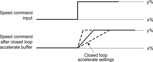
Closed-Loop Accelerate

To prevent sudden changes in the torque applied to the motor which could result in acoustic noise, the DRV10987 device provides the option of limiting the maximum rate at which the speed command changes. ClsLpAccel[2:0] can be programmed to set the maximum rate at which the speed command changes (shown in Figure 30).
DRV10987 closed_loop_accel_LVSCP2.gifFigure 30. Closed-Loop Accelerate