SLVSBA8G
March 2012 – March 2018
DRV110
PRODUCTION DATA.
1
Features
2
Applications
3
Description
Device Images
DRV110 Supplied by Power Line Voltage
4
Revision History
5
Pin Configuration and Functions
Pin Functions
6
Specifications
6.1
Absolute Maximum Ratings
6.2
ESD Ratings
6.3
Recommended Operating Conditions
6.4
Thermal Information
6.5
Electrical Characteristics
6.6
Typical Characteristics
7
Detailed Description
7.1
Overview
7.2
Functional Block Diagram
7.3
Feature Description
7.3.1
Keep Time
7.3.2
PWM Current Control
7.3.3
Configuring Peak and Hold Currents
7.3.4
Configuring the PWM Frequency
7.3.5
Voltage Supply and Integrated Zener Diode
7.4
Device Functional Modes
7.4.1
Normal Mode
7.4.2
Shutdown
8
Application and Implementation
8.1
Application Information
8.2
Typical Application
8.2.1
Design Requirements
8.2.2
Detailed Design Procedure
8.2.2.1
Current Limiting Resistor Selection
8.2.2.2
Passive Component Selection
8.2.3
Application Curve
9
Power Supply Recommendations
10
Layout
10.1
Layout Guidelines
10.2
Layout Example
11
Device and Documentation Support
11.1
Documentation Support
11.1.1
Related Documentation
11.2
Receiving Notification of Documentation Updates
11.3
Community Resources
11.4
Trademarks
11.5
Electrostatic Discharge Caution
11.6
Glossary
12
Mechanical, Packaging, and Orderable Information
Package Options
Mechanical Data (Package|Pins)
PW|8
MPDS568
PW|14
MPDS360A
Thermal pad, mechanical data (Package|Pins)
Orderable Information
slvsba8g_oa
slvsba8g_pm
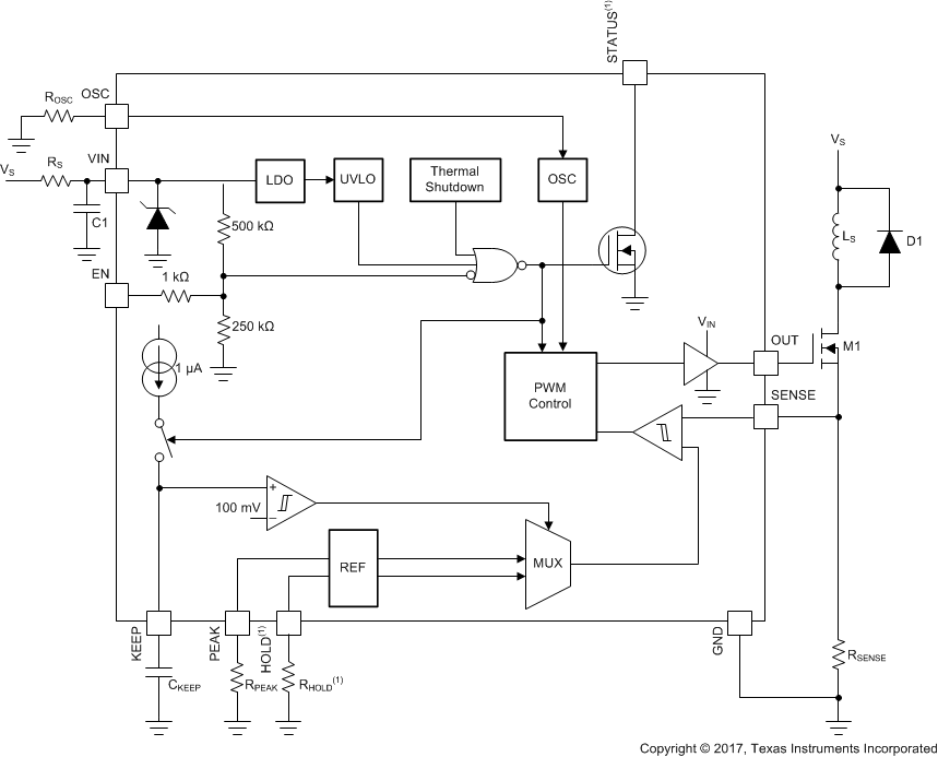
7.2
Functional Block Diagram
1.
Available only in the 14-pin package.