SLVSBG3C June 2012 – June 2016 DRV120
PRODUCTION DATA.
- 1 Features
- 2 Applications
- 3 Description
- 4 Revision History
- 5 Pin Configuration and Functions
- 6 Specifications
- 7 Detailed Description
- 8 Application and Implementation
- 9 Power Supply Recommendations
- 10Layout
- 11Device and Documentation Support
- 12Mechanical, Packaging, and Orderable Information
Package Options
Mechanical Data (Package|Pins)
Thermal pad, mechanical data (Package|Pins)
Orderable Information
8 Application and Implementation
NOTE
Information in the following applications sections is not part of the TI component specification, and TI does not warrant its accuracy or completeness. TI’s customers are responsible for determining suitability of components for their purposes. Customers should validate and test their design implementation to confirm system functionality.
8.1 Application Information
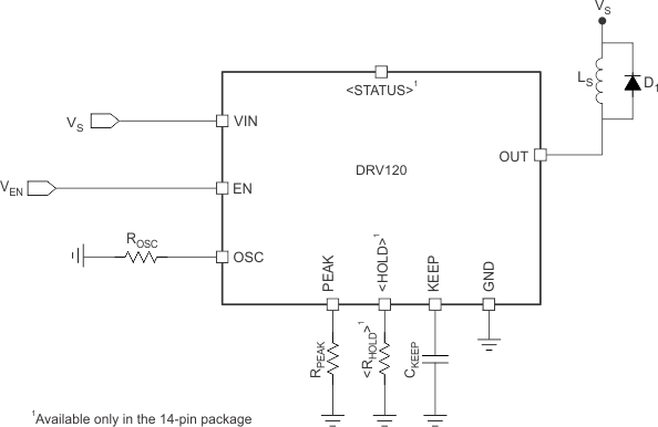
The DRV120 device is designed to operate a solenoid valve or relay. A typical DC input design will be outlined in Typical Application. Approximate resistor and capacitor values for the peak current, hold current, and keep time will be derived for a sample application.
8.2 Typical Application
 Figure 5. Default Configuration
8.2.1 Design Requirements
The key elements to identify here are the system input voltage, peak current, hold current, and peak keep time values required for the solenoid or relay being used. With these values, approximate RS, RPEAK, RHOLD (for 14-pin package), and CKEEP values can be determined and the proper FET and diode can be identified. ROSC can be varied in order to tune the circuit to the chosen solenoid or relay.
8.2.2 Detailed Design Procedure
First, with the known peak current, hold current, and peak keep time values known, the RPEAK, RHOLD (for 14-pin package), and CKEEP values can be determined. Calculation will proceed based on example values shown in Table 1.
Table 1. Sample Application Values
| VARIABLE | VALUE |
|---|---|
| Peak current | 150 mA |
| Hold current | 50 mA |
| Keep time | 100 ms |
RPEAK and RHOLD (if applicable) can be determined using Equation 2 and Equation 3. For the sample values, RPEAK is set to 111 kΩ and RHOLD can be shorted to GND. TI recommends that a 0-Ω resistor is used for prototyping in case changes to this value are desired.
Next, CKEEP can be set based on Equation 1, 1.33 µF for the sample values. ROSC can initially be shorted to GND, but again a 0-Ω resistor is recommended for prototyping. Additionally, a filter on the SENSE line may be added if it will be in a high-noise environment and is recommended for prototyping. Typical values for this are 1 kΩ and 100 pF.
Finally, a current recirculation diode must be chosen based on the current values defined in Table 1. The current recirculation diode should be a fast recovery diode.
8.2.3 Application Curves

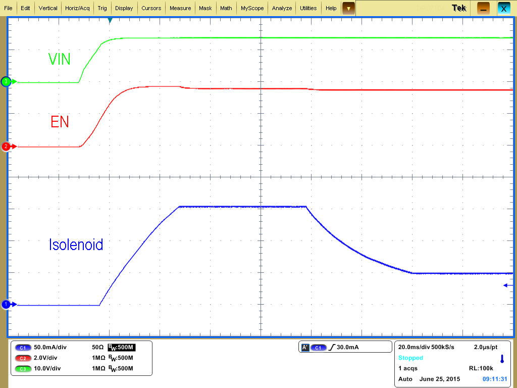
| Lind = 1 H | Rind = 50 Ω |