SLVSBG3C June 2012 – June 2016 DRV120
PRODUCTION DATA.
- 1 Features
- 2 Applications
- 3 Description
- 4 Revision History
- 5 Pin Configuration and Functions
- 6 Specifications
- 7 Detailed Description
- 8 Application and Implementation
- 9 Power Supply Recommendations
- 10Layout
- 11Device and Documentation Support
- 12Mechanical, Packaging, and Orderable Information
Package Options
Mechanical Data (Package|Pins)
Thermal pad, mechanical data (Package|Pins)
Orderable Information
7 Detailed Description
7.1 Overview
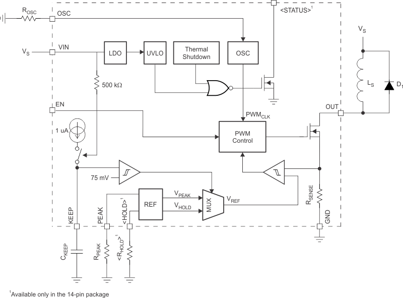
The DRV120 device provides a PWM current converter for use with solenoids. The device provides a quick ramp to a high peak current value in order to ensure opening of the valve or relay. The peak current is held for a programmable time and then released to a lower value to maintain the open state of the valve or relay while reducing the total current consumption. Peak current duration, peak current amount, hold current amount (in the 14-pin package), and PWM frequency can all be controlled by external components or used at default levels by omitting these components (except peak current duration). Enable and disable of the switch is controlled by the EN pin which has an internal pullup to VIN. The DRV120 also features a wide VIN range from 6 V to 28 V. Finally, the 14-pin package features an open-drain pulldown path on the STATUS pin which is enabled as long as undervoltage lockout or thermal shutdown has not triggered.
7.2 Functional Block Diagram

7.3 Feature Description
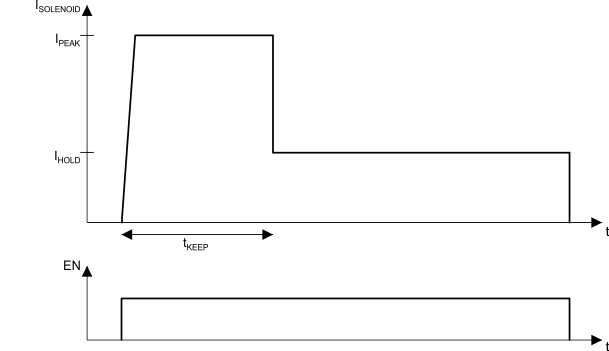
The DRV120 controls the current through the solenoid as shown in Figure 2. Activation starts when EN pin voltage is pulled high either by an external driver or internal pullup. In the beginning of activation, DRV120 allows the load current to ramp up to the peak value IPEAK and it regulates it at the peak value for the time, tKEEP, before reducing it to IHOLD. The load current is regulated at the hold value as long as the EN pin is kept high. The initial current ramp-up time depends on the inductance and resistance of the solenoid. Once EN pin is driven to GND, DRV120 allows the solenoid current to decay to zero.
 Figure 2. Typical Current Waveform Through the Solenoid
tKEEP is set externally by connecting a capacitor to the KEEP pin. A constant current is sourced from the KEEP pin that is driven into an external capacitor resulting in a linear voltage ramp. When the KEEP pin voltage reaches 75 mV, the current regulation reference voltage, VREF, is switched from VPEAK to VHOLD. Dependency of tKEEP from the external capacitor size can be calculated with Equation 1.

The current control loop regulates, cycle-by-cycle, the solenoid current by using an internal current-sensing resistor and MOSFET switch. During the ON-cycle, current flows from OUT pin to GND pin through the internal switch as long as voltage across the current-sensing resistor is less than VREF. As soon as the current sensing voltage is above VREF, the internal switch is immediately turned off until the next ON-cycle is triggered by the internal PWM clock signal. In the beginning of each ON-cycle, the internal switch is turned on and stays on for at least the time determined by the minimum PWM signal duty cycle, DMIN.
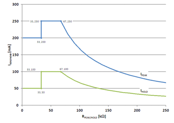
IPEAK and IHOLD depend on fixed resistance values RPEAK and RHOLD approximately as shown in Figure 3. If the PEAK pin is connected to ground or if RPEAK or RHOLD is below 33.33 kΩ (typical value), then IPEAK is at its default value (internal setting) of 200 mA for IPEAK and 50 mA for IHOLD. The IPEAK value can alternatively be set by connecting an external resistor to ground from the PEAK pin. For example, if a 50-kΩ (= RPEAK) resistor is connected between PEAK and GND, then the externally set IPEAK level will be 250 mA. If RPEAK = 200 kΩ is, then the externally set IPEAK level will be 83 mA. In the 8-pin package, IHOLD is set to 50 mA by default. In the 14-pin package, external settings of IHOLD works in the same way as IPEAK. External settings for IPEAK and IHOLD are independent of each other. Approximate IPEAK and IHOLD values can be calculated by using Equation 2 and Equation 3.


 Figure 3. PEAK and HOLD Mode Current Settings
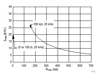
Frequency of the internal PWM clock signal, PWMCLK, that triggers each ON-cycle can be adjusted by external resistor, ROSC, connected between OSC and GND. Frequency as a function of resistor value is shown in Figure 4. Default frequency is used when OSC is connected to GND directly. Use Equation 4 to calculate the PWM frequency as a function of the external fixed adjustment resistor value (greater than 160 kΩ).

Open-drain STATUS output is deactivated if either undervoltage lockout or thermal shutdown blocks have triggered.
7.4 Device Functional Modes
The DRV120 transitions through three different states. The first is the OFF state, where the EN pin is low and the PWM output is off. The second is the PEAK state, which begins when the EN pin is pulled high by an external controller or internal pullup, and ends once tKEEP has been reached. During this state, the PWM operates in order to reach the IPEAK set by the RPEAK. Finally, once tKEEP has been reached, the PWM continues to operate, but at the IHOLD level. This continues until the EN pin is forced low again and the PWM turns off.
