SLOS919D June   2016  – November 2023 DRV2510-Q1

PRODUCTION DATA  

  1.   1
  2. Features
  3. Applications
  4. Description
  5. Revision History
  6. Pin Configuration and Functions
  7. Specifications
    1. 6.1 Absolute Maximum Ratings
    2. 6.2 ESD Ratings
    3. 6.3 Recommended Operating Conditions
    4. 6.4 Thermal Information
    5. 6.5 Electrical Characteristics
    6. 6.6 Timing Requirements
    7. 6.7 Switching Characteristics
    8. 6.8 Typical Characteristics
  8. Detailed Description
    1. 7.1 Overview
    2. 7.2 Functional Block Diagram
    3. 7.3 Feature Description
      1. 7.3.1 Analog Input and Configurable Pre-amplifier
      2. 7.3.2 Pulse-Width Modulator (PWM)
      3. 7.3.3 Designed for low EMI
      4. 7.3.4 Device Protection Systems
        1. 7.3.4.1 Diagnostics
          1. 7.3.4.1.1 Load Diagnostics
        2. 7.3.4.2 Faults During Load Diagnostics
        3. 7.3.4.3 Protection and Monitoring
    4. 7.4 Device Functional Modes
      1. 7.4.1 Operation in Shutdown Mode
      2. 7.4.2 Operation in Standby Mode
      3. 7.4.3 Operation in Active Mode
    5. 7.5 Programming
      1. 7.5.1 General I2C Operation
      2. 7.5.2 Single-Byte and Multiple-Byte Transfers
      3. 7.5.3 Single-Byte Write
      4. 7.5.4 Multiple-Byte Write and Incremental Multiple-Byte Write
      5. 7.5.5 Single-Byte Read
      6. 7.5.6 Multiple-Byte Read
    6. 7.6 Register Map
      1. 7.6.1 Address: 0x01
      2. 7.6.2 Address: 0x02
      3. 7.6.3 Address: 0x03
  9. Application and Implementation
    1. 8.1 Application Information
    2. 8.2 Typical Applications
      1. 8.2.1 Single-Ended Source
        1. 8.2.1.1 Design Requirements
        2. 8.2.1.2 Detailed Design Procedure
          1. 8.2.1.2.1 Optional Components
          2. 8.2.1.2.2 Capacitor Selection
          3. 8.2.1.2.3 Solenoid Selection
          4. 8.2.1.2.4 Output Filter Considerations
        3. 8.2.1.3 Application Curves
        4. 8.2.1.4 Differential Input Diagram
  10. Power Supply Recommendations
  11. 10Layout
    1. 10.1 Layout Guidelines
    2. 10.2 Layout Example
  12. 11Device and Documentation Support
    1. 11.1 Device Support
      1. 11.1.1 Third-Party Products Disclaimer
    2. 11.2 Receiving Notification of Documentation Updates
    3. 11.3 Support Resources
    4. 11.4 Trademarks
    5. 11.5 Electrostatic Discharge Caution
    6. 11.6 Glossary
  13. 12Mechanical, Packaging, and Orderable Information

Package Options

Mechanical Data (Package|Pins)
Thermal pad, mechanical data (Package|Pins)
Orderable Information

Application Curves

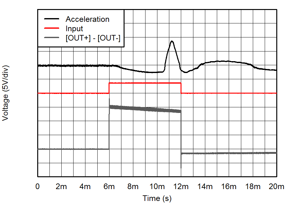
These application curves were taken using an HA200 solenoid with a 100-g mass, and the acceleration was measured using the DRV-AAC16-EVM accelerometer. The following scales apply to the graphs:

  • Output Differential Voltage scale is shown on the plots at 5-V/div
  • Acceleration scale is 5.85-G/div
  • Current scale is 2-A/div

GUID-1E551716-B4D3-4D3A-AF49-D86898E3EF83-low.pngFigure 8-2 Voltage and Acceleration vs Time (Input Square Wave)
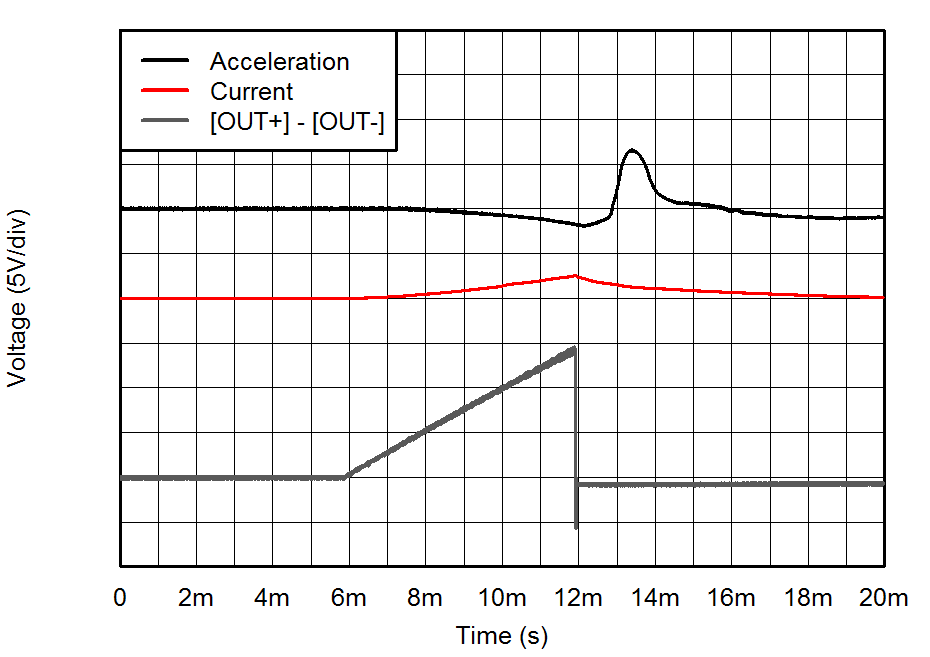
GUID-489BFB28-BC39-4B44-A98E-C36D787B6C36-low.pngFigure 8-4 Voltage and Acceleration vs Time (Ramp Wave)
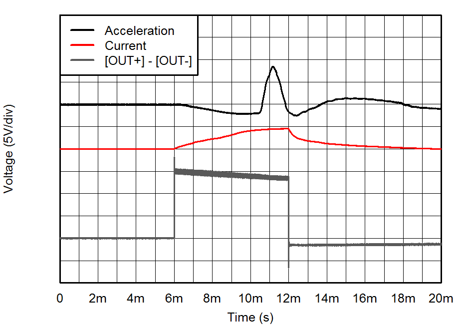
GUID-CE61CFB7-2AA9-4D41-8864-F727D50502C9-low.pngFigure 8-3 Voltage and Acceleration vs Time (Square Wave)
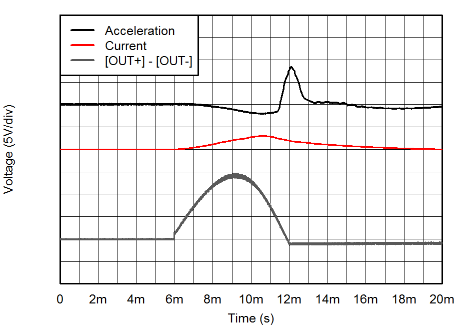
GUID-C8E9C7CB-B43B-4E16-BECA-D9FB1C2095BE-low.pngFigure 8-5 Voltage and Acceleration vs Time (1/2 Sine Wave)