SLOS916B June   2016  – June 2020 DRV2511-Q1

PRODUCTION DATA.  

  1. Features
  2. Applications
  3. Description
    1.     Simplified Schematic
  4. Revision History
  5. Pin Configuration and Functions
    1.     Pin Functions
  6. Specifications
    1. 6.1 Absolute Maximum Ratings
    2. 6.2 ESD Ratings
    3. 6.3 Recommended Operating Conditions
    4. 6.4 Thermal Information
    5. 6.5 Electrical Characteristics
    6. 6.6 Switching Characteristics
    7. 6.7 Typical Characteristics
  7. Detailed Description
    1. 7.1 Overview
    2. 7.2 Functional Block Diagram
    3. 7.3 Feature Description
      1. 7.3.1 Analog Input and Configurable Pre-amplifier
      2. 7.3.2 Pulse-Width Modulator (PWM)
      3. 7.3.3 Designed for low EMI
      4. 7.3.4 Device Protection Systems
    4. 7.4 Device Functional Modes
      1. 7.4.1 Operation in Shutdown Mode
      2. 7.4.2 Operation in Standby Mode
      3. 7.4.3 Operation in Active Mode
  8. Programming
    1. 8.1 Gain
  9. Application and Implementation
    1. 9.1 Application Information
    2. 9.2 Typical Application, Single Ended Input
      1. 9.2.1 Design Requirements
      2. 9.2.2 Detailed Design Procedure
        1. 9.2.2.1 Optional Components
        2. 9.2.2.2 Capacitor Selection
        3. 9.2.2.3 Solenoid Selection
        4. 9.2.2.4 Output Filter Considerations
      3. 9.2.3 Application Curves
      4. 9.2.4 Typical Application, Differential Input
  10. 10Power Supply Recommendations
    1. 10.1 Power Dissipation and Maximum Ambient Temperature
  11. 11Layout
    1. 11.1 Layout Guidelines
    2. 11.2 Layout Example
  12. 12Device and Documentation Support
    1. 12.1 Documentation Support
    2. 12.2 Receiving Notification of Documentation Updates
    3. 12.3 Community Resources
    4. 12.4 Trademarks
    5. 12.5 Electrostatic Discharge Caution
    6. 12.6 Glossary
  13. 13Mechanical, Packaging, and Orderable Information

Package Options

Mechanical Data (Package|Pins)
Thermal pad, mechanical data (Package|Pins)
Orderable Information

Description

The DRV2511-Q1 device is a high current haptic driver specifically designed for inductive loads, such as solenoids and voice coils.

The output stage of the DRV2511-Q1 device consists of a full H-bridge capable of delivering 8 A of peak current.

The DRV2511-Q1 device provides protection functions such as undervoltage lockout, over-current protection and over-temperature protection.

The DRV2511-Q1 device is automotive qualified.

Device Information(1)

PART NUMBER PACKAGE BODY SIZE (NOM)
DRV2511-Q1 HTSSOP (32) 11.00 mm × 6.20 mm
  1. For all available packages, see the orderable addendum at the end of the data sheet.

Simplified Schematic
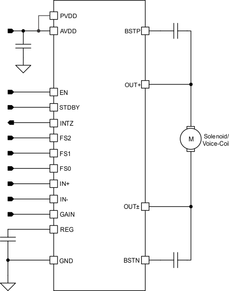
DRV2511-Q1 fp_circuit_slos916.gif