SLOS754C June 2012 – August 2016 DRV2603
PRODUCTION DATA.
- 1 Features
- 2 Applications
- 3 Description
- 4 Revision History
- 5 Pin Configuration and Functions
- 6 Specifications
- 7 Parameter Measurement Information
-
8 Detailed Description
- 8.1 Overview
- 8.2 Functional Block Diagram
- 8.3
Feature Description
- 8.3.1 Supply Voltage Rejection for Constant Vibration Strength
- 8.3.2 Low-Voltage Control Logic for Constant Vibration Strength
- 8.3.3 Thermal Protection
- 8.3.4 Overcurrent Protection
- 8.3.5 Linear Resonance Actuators (LRA)
- 8.3.6 Auto Resonance Engine for LRA
- 8.3.7 Eccentric Rotating Mass Motors (ERM)
- 8.3.8 Edge Rate Control
- 8.4 Device Functional Modes
- 9 Application and Implementation
- 10Power Supply Recommendations
- 11Layout
- 12Device and Documentation Support
- 13Mechanical, Packaging, and Orderable Information
Package Options
Mechanical Data (Package|Pins)
- RUN|10
Thermal pad, mechanical data (Package|Pins)
- RUN|10
Orderable Information
6 Specifications
6.1 Absolute Maximum Ratings(1)
over operating free-air temperature range, TA = 25°C (unless otherwise noted)| MIN | MAX | UNIT | |||
|---|---|---|---|---|---|
| Supply voltage | VDD | –0.3 | 6 | V | |
| VI | Input voltage | EN, PWM, LRA/ERM | –0.3 | VDD + 0.3 | V |
| TA | Operating free-air temperature range | –40 | 85 | °C | |
| TJ | Operating junction temperature range | –40 | 150 | °C | |
| Tstg | Storage temperature range | –65 | 150 | °C | |
(1) Stresses beyond those listed under Absolute Maximum Ratings may cause permanent damage to the device. These are stress ratings only, which do not imply functional operation of the device at these or any other conditions beyond those indicated under Recommended Operating Conditions. Exposure to absolute-maximum-rated conditions for extended periods may affect device reliability.
6.2 ESD Ratings
| VALUE | UNIT | |||
|---|---|---|---|---|
| V(ESD) | Electrostatic discharge | Human body model (HBM), per ANSI/ESDA/JEDEC JS-001(1) | ±2000 | V |
| Charged-device model (CDM), per JEDEC specification JESD22-C101(2) | ±500 | |||
(1) JEDEC document JEP155 states that 500-V HBM allows safe manufacturing with a standard ESD control process.
(2) JEDEC document JEP157 states that 250-V CDM allows safe manufacturing with a standard ESD control process.
6.3 Recommended Operating Conditions
| MIN | TYP | MAX | UNIT | |||
|---|---|---|---|---|---|---|
| VDD | Supply voltage | VDD | 2.5 | 5.2 | V | |
| fPWM | PWM Input frequency | 10 | 250 | kHz | ||
| RL | Load Impedance | VDD = 5.2 V | 8 | Ω | ||
| F0 | Supported LRA frequency | Auto resonance tracking range for LRA | 140 | 220 | Hz | |
| VIL | Digital input low voltage | EN, PWM, LRA/ERM | 0.6 | V | ||
| VIH | Digital input high voltage | EN, PWM, LRA/ERM | 1.2 | V | ||
| TA | Operating free-air temperature range | -40 | 85 | °C | ||
6.4 Thermal Information
| THERMAL METRIC(1) | DRV2603 | UNIT | |
|---|---|---|---|
| RUN (WQFN) | |||
| 10 PINS | |||
| RθJA | Junction-to-ambient thermal resistance | 153.7 | °C/W |
| RθJC(top) | Junction-to-case (top) thermal resistance | 86 | °C/W |
| RθJB | Junction-to-board thermal resistance | 70.4 | °C/W |
| ψJT | Junction-to-top characterization parameter | 1.3 | °C/W |
| ψJB | Junction-to-board characterization parameter | 70.4 | °C/W |
(1) For more information about traditional and new thermal metrics, see the Semiconductor and IC Package Thermal Metrics application report.
6.5 Electrical Characteristics
TA = 25°C, VDD = 3.6 V (unless otherwise noted)| PARAMETER | TEST CONDITIONS | MIN | TYP | MAX | UNIT | ||
|---|---|---|---|---|---|---|---|
| |IIL| | Digital input low current | EN, PWM, LRA/ERM | VDD = 5.0 V, VIN = 0 V | 1 | µA | ||
| |IIH| | Digital input high current | EN | VDD = 5.0 V, VIN = VDD | 6 | µA | ||
| PWM, LRA/ERM | VDD = 5.0 V, VIN = VDD | 3 | µA | ||||
| ISD | Shut down current | VEN = 0 V | 0.3 | 3 | µA | ||
| IDDQ | Quiescent current | VEN = VDD, ERM Mode, 50% duty cycle input, No load | 1.7 | 2.5 | mA | ||
| ROUT | Output impedance in shutdown | OUT+ to GND, OUT– to GND | 15 | kΩ | |||
| tSU | Start-up time | Time from EN high to output signal | 1.3 | ms | |||
| fSW | PWM output frequency | 19.5 | 20.3 | 21.5 | kHz | ||
| IBAT,AVG | Average battery current during operation | Duty Cycle = 100%, LRA Mode, Load = 25 Ω LRA | 55 | mA | |||
| Duty Cycle = 80%, ERM Mode, RL = 17 Ω, 2V rated ERM | 59 | ||||||
| RDS-HS | Drain to source resistance, high-side | 1.05 | Ω | ||||
| RDS-LS | Drain to source resistance, low-side | 0.85 | Ω | ||||
| VOUT | Differential output voltage | Duty Cycle = 100%, LRA Mode, Load = 25 Ω LRA | 2.2 | VRMS | |||
| Duty Cycle = 100%, ERM Mode, RL = 20 Ω ERM | 3.3 | V | |||||
| Thermal threshold | 145 | °C | |||||
| Thermal Hysteresis | 18 | °C | |||||
6.6 Typical Characteristics
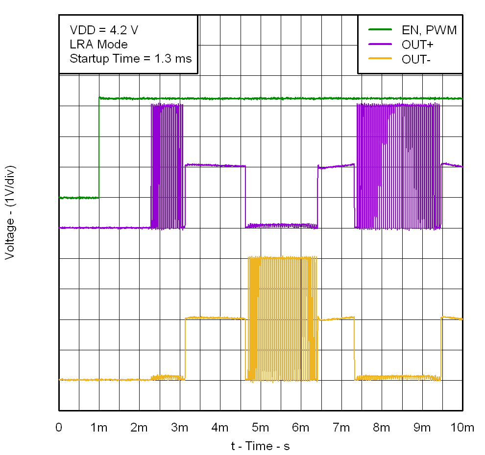 Figure 1. Startup Waveform
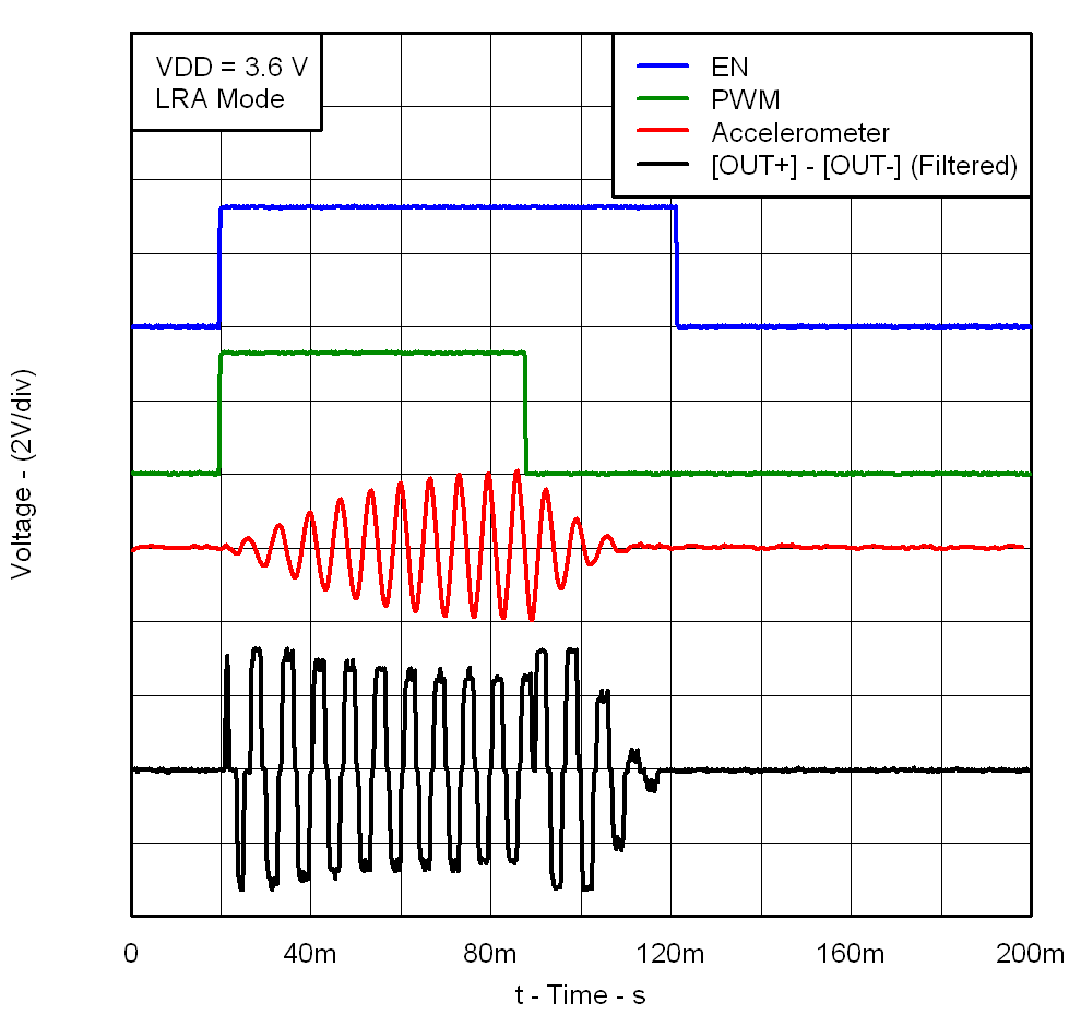 Figure 3. LRA Click
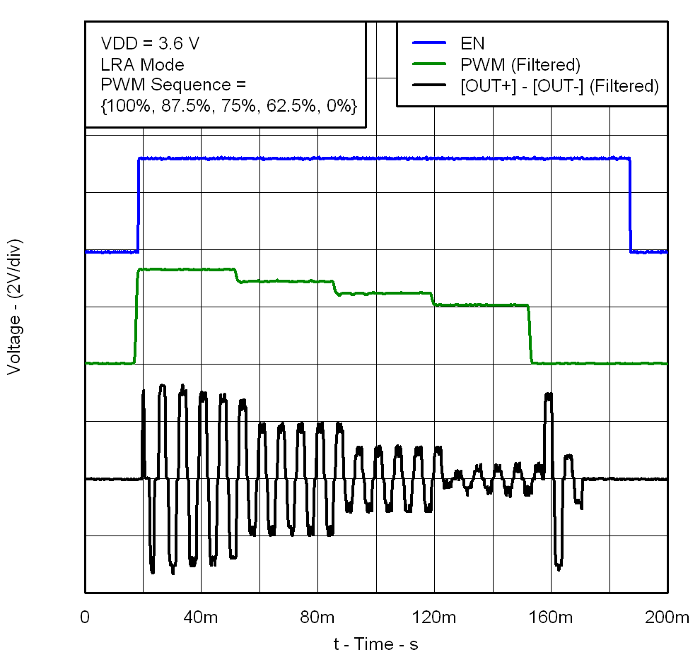 Figure 5. LRA PWM Modulation
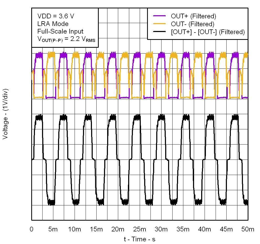 Figure 2. LRA Full-Scale Drive
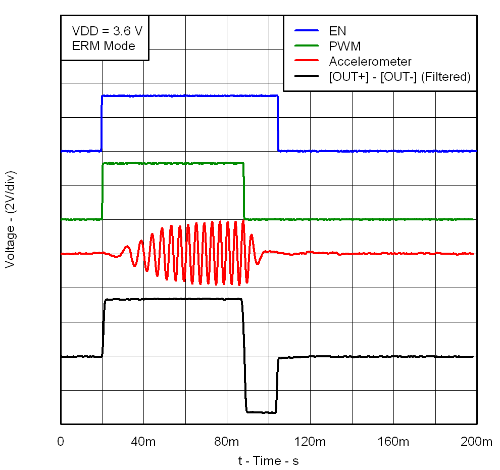 Figure 4. ERM Click
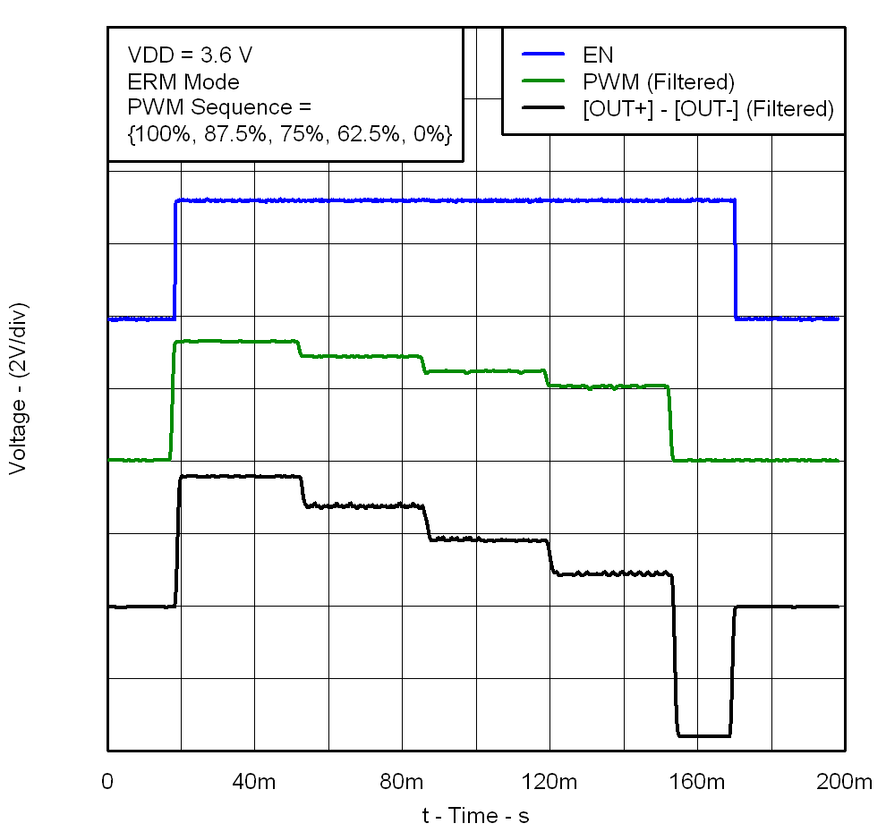 Figure 6. ERM PWM Modulation