SLOS824C December   2012  – March 2018 DRV2604

PRODUCTION DATA.  

  1. Features
  2. Applications
  3. Description
    1.     Simplified Schematic
  4. Revision History
  5. Pin Configuration and Functions
    1.     Pin Functions
  6. Specifications
    1. 6.1 Absolute Maximum Ratings
    2. 6.2 ESD Ratings
    3. 6.3 Recommended Operating Conditions
    4. 6.4 Thermal Information
    5. 6.5 Electrical Characteristics
    6. 6.6 Timing Requirements
    7. 6.7 Switching Characteristics
    8. 6.8 Typical Characteristics
  7. Detailed Description
    1. 7.1 Overview
    2. 7.2 Functional Block Diagram
    3. 7.3 Feature Description
      1. 7.3.1  Support for ERM and LRA Actuators
      2. 7.3.2  Smart-Loop Architecture
        1. 7.3.2.1 Auto-Resonance Engine for LRA
        2. 7.3.2.2 Real-Time Resonance-Frequency Reporting for LRA
        3. 7.3.2.3 Automatic Overdrive and Braking
          1. 7.3.2.3.1 Startup Boost
          2. 7.3.2.3.2 Brake Factor
          3. 7.3.2.3.3 Brake Stabilizer
        4. 7.3.2.4 Automatic Level Calibration
          1. 7.3.2.4.1 Automatic Compensation for Resistive Losses
          2. 7.3.2.4.2 Automatic Back-EMF Normalization
          3. 7.3.2.4.3 Calibration Time Adjustment
          4. 7.3.2.4.4 Loop-Gain Control
          5. 7.3.2.4.5 Back-EMF Gain Control
        5. 7.3.2.5 Actuator Diagnostics
      3. 7.3.3  Open-Loop Operation for LRA
      4. 7.3.4  Open-Loop Operation for ERM
      5. 7.3.5  Flexible Front-End Interface
        1. 7.3.5.1 PWM Interface
        2. 7.3.5.2 Internal Memory Interface
          1. 7.3.5.2.1 Waveform Sequencer
          2. 7.3.5.2.2 Library Parameterization
        3. 7.3.5.3 Real-Time Playback (RTP) Interface
        4. 7.3.5.4 Analog Input Interface
        5. 7.3.5.5 Input Trigger Option
          1. 7.3.5.5.1 I2C Trigger
          2. 7.3.5.5.2 Edge Trigger
          3. 7.3.5.5.3 Level Trigger
        6. 7.3.5.6 Noise Gate Control
      6. 7.3.6  Edge Rate Control
      7. 7.3.7  Constant Vibration Strength
      8. 7.3.8  Battery Voltage Reporting
      9. 7.3.9  One-Time Programmable (OTP) Memory for Configuration
      10. 7.3.10 Low-Power Standby
      11. 7.3.11 Device Protection
        1. 7.3.11.1 Thermal Protection
        2. 7.3.11.2 Overcurrent Protection of the Actuator
    4. 7.4 Device Functional Modes
      1. 7.4.1 Power States
        1. 7.4.1.1 Operation With VDD < 2.5 V (Minimum VDD)
        2. 7.4.1.2 Operation With VDD > 6 V (Absolute Maximum VDD)
        3. 7.4.1.3 Operation With EN Control
        4. 7.4.1.4 Operation With STANDBY Control
        5. 7.4.1.5 Operation With DEV_RESET Control
        6. 7.4.1.6 Operation in the Active State
      2. 7.4.2 Changing Modes of Operation
      3. 7.4.3 Operation of the GO Bit
      4. 7.4.4 Operation During Exceptional Conditions
        1. 7.4.4.1 Operation With No Actuator Attached
        2. 7.4.4.2 Operation With a Short at REG Pin
        3. 7.4.4.3 Operation With a Short at OUT+, OUT–, or Both
    5. 7.5 Programming
      1. 7.5.1 Auto-Resonance Engine Programming for the LRA
        1. 7.5.1.1 Drive-Time Programming
        2. 7.5.1.2 Current-Dissipation Time Programming
        3. 7.5.1.3 Blanking Time Programming
      2. 7.5.2 Automatic-Level Calibration Programming
        1. 7.5.2.1 Rated Voltage Programming
        2. 7.5.2.2 Overdrive Voltage-Clamp Programming
      3. 7.5.3 I2C Interface
        1. 7.5.3.1 TI Haptic Broadcast Mode
        2. 7.5.3.2 General I2C Operation
        3. 7.5.3.3 Single-Byte and Multiple-Byte Transfers
        4. 7.5.3.4 Single-Byte Write
        5. 7.5.3.5 Multiple-Byte Write and Incremental Multiple-Byte Write
        6. 7.5.3.6 Single-Byte Read
        7. 7.5.3.7 Multiple-Byte Read
      4. 7.5.4 Programming for Open-Loop Operation
        1. 7.5.4.1 Programming for ERM Open-Loop Operation
        2. 7.5.4.2 Programming for LRA Open-Loop Operation
      5. 7.5.5 Programming for Closed-Loop Operation
      6. 7.5.6 Auto Calibration Procedure
      7. 7.5.7 Programming On-Chip OTP Memory
      8. 7.5.8 Waveform Playback Programming
        1. 7.5.8.1 Data Formats for Waveform Playback
          1. 7.5.8.1.1 Open-Loop Mode
          2. 7.5.8.1.2 Closed-Loop Mode, Unidirectional
          3. 7.5.8.1.3 Closed-Loop Mode, Bidirectional
        2. 7.5.8.2 Waveform Setup and Playback
          1. 7.5.8.2.1 Waveform Playback Using RTP Mode
          2. 7.5.8.2.2 Waveform Playback Using the Analog-Input Mode
          3. 7.5.8.2.3 Waveform Playback Using PWM Mode
          4. 7.5.8.2.4 Loading Data to RAM
            1. 7.5.8.2.4.1 Header Format
            2. 7.5.8.2.4.2 RAM Waveform Data Format
          5. 7.5.8.2.5 Waveform Sequencer
          6. 7.5.8.2.6 Waveform Triggers
    6. 7.6 Register Map
      1. 7.6.1  Status (Address: 0x00)
        1. Table 3. Status Register Field Descriptions
      2. 7.6.2  Mode (Address: 0x01)
        1. Table 4. Mode Register Field Descriptions
      3. 7.6.3  Real-Time Playback Input (Address: 0x02)
        1. Table 5. Real-Time Playback Input Register Field Descriptions
      4. 7.6.4  HI_Z (Address: 0x03)
        1. Table 6. HI_Z Register Field Descriptions
      5. 7.6.5  Waveform Sequencer (Address: 0x04 to 0x0B)
        1. Table 7. Waveform Sequencer Register Field Descriptions
      6. 7.6.6  GO (Address: 0x0C)
        1. Table 8. GO Register Field Descriptions
      7. 7.6.7  Overdrive Time Offset (Address: 0x0D)
        1. Table 9. Overdrive Time Offset Register Field Descriptions
      8. 7.6.8  Sustain Time Offset, Positive (Address: 0x0E)
        1. Table 10. Sustain Time Offset, Positive Register Field Descriptions
      9. 7.6.9  Sustain Time Offset, Negative (Address: 0x0F)
        1. Table 11. Sustain Time Offset, Negative Register Field Descriptions
      10. 7.6.10 Brake Time Offset (Address: 0x10)
        1. Table 12. Brake Time Offset Register Field Descriptions
      11. 7.6.11 Rated Voltage (Address: 0x16)
        1. Table 13. Rated Voltage Register Field Descriptions
      12. 7.6.12 Overdrive Clamp Voltage (Address: 0x17)
        1. Table 14. Overdrive Clamp Voltage Register Field Descriptions
      13. 7.6.13 Auto-Calibration Compensation Result (Address: 0x18)
        1. Table 15. Auto-Calibration Compensation-Result Register Field Descriptions
      14. 7.6.14 Auto-Calibration Back-EMF Result (Address: 0x19)
        1. Table 16. Auto-Calibration Back-EMF Result Register Field Descriptions
      15. 7.6.15 Feedback Control (Address: 0x1A)
        1. Table 17. Feedback Control Register Field Descriptions
      16. 7.6.16 Control1 (Address: 0x1B)
        1. Table 18. Control1 Register Field Descriptions
      17. 7.6.17 Control2 (Address: 0x1C)
        1. Table 19. Control2 Register Field Descriptions
      18. 7.6.18 Control3 (Address: 0x1D)
        1. Table 20. Control3 Register Field Descriptions
      19. 7.6.19 Control4 (Address: 0x1E)
        1. Table 21. Control4 Register Field Descriptions
      20. 7.6.20 V(BAT) Voltage Monitor (Address: 0x21)
        1. Table 22. V(BAT) Voltage-Monitor Register Field Descriptions
      21. 7.6.21 LRA Resonance Period (Address: 0x22)
        1. Table 23. LRA Resonance-Period Register Field Descriptions
      22. 7.6.22 RAM-Address Upper Byte (Address: 0xFD)
        1. Table 24. RAM-Address Upper-Byte Register Field Descriptions
      23. 7.6.23 RAM-Address Lower Byte (Address: 0xFE)
        1. Table 25. RAM Address Lower Byte Register Field Descriptions
      24. 7.6.24 RAM Data Byte (Address: 0xFF)
        1. Table 26. RAM-Data Byte Register Field Descriptions
  8. Application and Implementation
    1. 8.1 Application Information
    2. 8.2 Typical Application
      1. 8.2.1 Design Requirements
      2. 8.2.2 Detailed Design Procedure
        1. 8.2.2.1 Actuator Selection
          1. 8.2.2.1.1 Eccentric Rotating-Mass Motors (ERM)
          2. 8.2.2.1.2 Linear Resonance Actuators (LRA)
            1. 8.2.2.1.2.1 Auto-Resonance Engine for LRA
        2. 8.2.2.2 Capacitor Selection
        3. 8.2.2.3 Interface Selection
        4. 8.2.2.4 Power Supply Selection
      3. 8.2.3 Application Curves
    3. 8.3 Initialization Setup
      1. 8.3.1 Initialization Procedure
      2. 8.3.2 Typical Usage Examples
        1. 8.3.2.1 Play a Waveform or Waveform Sequence from the RAM Waveform Memory
        2. 8.3.2.2 Play a Real-Time Playback (RTP) Waveform
        3. 8.3.2.3 Play a PWM or Analog Input Waveform
  9. Power Supply Recommendations
  10. 10Layout
    1. 10.1 Layout Guidelines
      1. 10.1.1 Trace Width
    2. 10.2 Layout Example
  11. 11Device and Documentation Support
    1. 11.1 Documentation Support
      1. 11.1.1 Related Documentation
    2. 11.2 Receiving Notification of Documentation Updates
    3. 11.3 Community Resources
    4. 11.4 Trademarks
    5. 11.5 Electrostatic Discharge Caution
    6. 11.6 Glossary
  12. 12Mechanical, Packaging, and Orderable Information

Package Options

Mechanical Data (Package|Pins)
Thermal pad, mechanical data (Package|Pins)
Orderable Information

Operation of the GO Bit

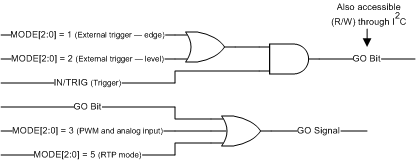
The GO bit is the primary way to assert the GO signal, which fires processes in the DRV2604 device. The primary purpose of the GO bit is to fire the playback of the waveform identifiers in the waveform sequencer (registers 0x04 to 0x0B). However, The GO bit can also fire the calibration or diagnostics processes.

When using the GO bit to play waveforms in internal trigger mode, the GO bit is asserted by writing 0x01 to register 0x0C. In this case, the GO bit can be thought of as a software trigger for haptic waveforms. The GO bit remains high until the playback of the haptic waveform sequence is complete. Clearing the GO bit during waveform playback cancels the waveform sequence. The GO bit can also be asserted by the external trigger when in external trigger mode. The GO bit in register 0x0C mirrors the state of the external trigger.

Setting RTP mode or PWM mode also sets the GO bit. However, setting the GO bit in this way has no impact on the GO bit located in register 0x0C.
DRV2604 goBit_slos866.gifFigure 16. GO-Signal Logic