SBOS814 December 2016 DRV401-Q1
PRODUCTION DATA.
- 1 Features
- 2 Applications
- 3 Description
- 4 Revision History
- 5 Pin Configuration and Functions
- 6 Specifications
-
7 Detailed Description
- 7.1 Overview
- 7.2 Functional Block Diagram
- 7.3
Feature Description
- 7.3.1 Magnetic Probe (Sensor) Interface
- 7.3.2 PWM Processing
- 7.3.3 Compensation Driver
- 7.3.4 External Compensation Coil Driver
- 7.3.5 Shunt Sense Amplifier
- 7.3.6 Over-Range Comparator
- 7.3.7 Voltage Reference
- 7.3.8 Demagnetization
- 7.3.9 Power-On and Brownout
- 7.3.10 Error Conditions
- 7.3.11 Protection Recommendations
- 7.4 Device Functional Modes
- 8 Application and Implementation
- 9 Power Supply Recommendations
- 10Layout
- 11Device and Documentation Support
- 12Mechanical, Packaging, and Orderable Information
Package Options
Mechanical Data (Package|Pins)
- RGW|20
Thermal pad, mechanical data (Package|Pins)
- RGW|20
Orderable Information
6 Specifications
6.1 Absolute Maximum Ratings
over operating free-air temperature range (unless otherwise noted).(1)| MIN | MAX | UNIT | ||
|---|---|---|---|---|
| Voltage | Supply voltage | 7 | V | |
| Signal input pin | −0.5 | VDD + 0.5 | ||
| Differential amplifier | Signal input pin | –10 | 10 | |
| Current | Signal input pin, IS1 and IS2 | –75 | 75 | mA |
| Pins other than IS1 and IS2 | –25 | 25 | ||
| ICOMP short circuit | 0 | 250 | ||
| Temperature | Operating, TA | –50 | 150 | °C |
| Junction, TJ | 150 | |||
| Storage, Tstg | –55 | 150 | ||
(1) Stresses beyond those listed under Absolute Maximum Ratings may cause permanent damage to the device. These are stress ratings only, which do not imply functional operation of the device at these or any other conditions beyond those indicated under Recommended Operating Conditions. Exposure to absolute-maximum-rated conditions for extended periods may affect device reliability.
6.2 ESD Ratings
| VALUE | UNIT | ||||
|---|---|---|---|---|---|
| V(ESD) | Electrostatic discharge | Human-body model (HBM), per AEC Q100-002 (1) | Pins IAIN1 and IAIN2 | ±1000 | V |
| All other pins | ±5000 | ||||
| Charged-device model (CDM), per AEC Q100-011 | All pins | ±1000 | |||
| Corner pins | ±1000 | ||||
(1) AEC Q100-002 indicates that HBM stressing shall be in accordance with the ANSI/ESDA/JEDEC JS-001 specification
6.3 Recommended Operating Conditions
over operating free-air temperature range (unless otherwise noted)| MIN | NOM | MAX | UNIT | ||
|---|---|---|---|---|---|
| Power supply voltage, VDD1, VDD2 | 4.5 | 5 | 5.5 | V | |
| Specified temperature range | –40 | 25 | +125 | °C | |
6.4 Thermal Information
over operating free-air temperature range (unless otherwise noted)| THERMAL METRIC(1) | DRV401-Q1 | UNIT | |
|---|---|---|---|
| RGW (VQFN) |
|||
| 20 PINS | |||
| RθJA | Junction-to-ambient thermal resistance | 34.1 | °C/W |
| RθJC(top) | Junction-to-case (top) thermal resistance | 22.8 | °C/W |
| RθJB | Junction-to-board thermal resistance | 12.1 | °C/W |
| ψJT | Junction-to-top characterization parameter | 0.3 | °C/W |
| ψJB | Junction-to-board characterization parameter | 12.0 | °C/W |
| RθJC(bot) | Junction-to-case (bottom) thermal resistance | 3.5 | °C/W |
(1) For more information about traditional and new thermal metrics, see the Semiconductor and IC Package Thermal Metrics application report.
6.5 Electrical Characteristics
at TA = 25°C and VDD1 = VDD2 = 5 V with external 100-kHz filter bandwidth (unless otherwise noted)| PARAMETER | TEST CONDITIONS | MIN | TYP | MAX | UNIT | |
|---|---|---|---|---|---|---|
| DIFFERENTIAL AMPLIFIER | ||||||
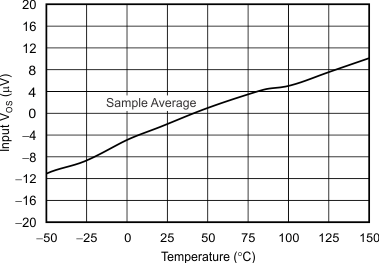
| VOS | Offset voltage, RTO(1)(2) | RL = 10 kΩ to 2.5 V VREFIN = 2.5 V Gain = 4 V/V |
±0.01 | ±0.1 | mV | |
| dVOS/dT | Offset voltage drift, RTO(2) | RL = 10 kΩ to 2.5 V VREFIN = 2.5 V TA = –40°C to 125°C ICOMP = 0 mA |
±0.1 | ±1 | µV/°C | |
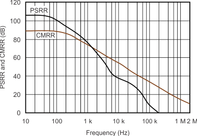
| CMRR | Offset voltage vs common-mode, RTO | RL = 10 kΩ to 2.5 V VREFIN = 2.5 V −1 V to 6 V, VREF = 2.5 V |
±50 | ±250 | µV/V | |
| PSRR | Offset voltage vs power supply, RTO | RL = 10 kΩ to 2.5 V VREFIN = 2.5 V VREF not included |
±4 | ±50 | µV/V | |
| SIGNAL INPUT | ||||||
| Common-mode voltage range | RL = 10 kΩ to 2.5 V VREFIN = 2.5 V |
–1 | (VDD) + 1 | V | ||
| SIGNAL OUTPUT | ||||||
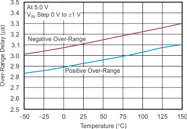
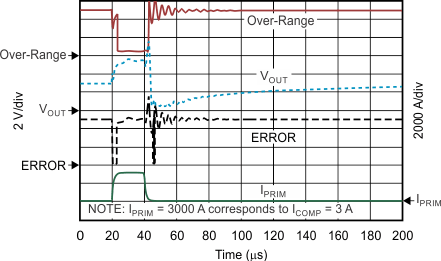
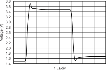
| Signal overrange indication (OVER-RANGE), delay(2) | RL = 10 kΩ to 2.5 V, VREFIN = 2.5 V, TA = –40°C to 125°C, ICOMP = 0 mA, VIN = 1-V step. See (2) |
2.5 to 3.5 | µs | |||
| Voltage output swing from negative rail(2), OVER-RANGE trip level |
RL = 10 kΩ to 2.5 V VREFIN = 2.5 V I = 2.5 mA, CMP trip level |
48 | 85 | mV | ||
| Voltage output swing from positive rail(2), OVER-RANGE trip level |
RL = 10 kΩ to 2.5 V VREFIN = 2.5 V I = −2.5 mA, CMP trip level |
VDD – 85 | VDD – 48 | mV | ||
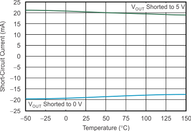
| ISC | Short-circuit current(2) | RL = 10 kΩ to 2.5 V VREFIN = 2.5 V VOUT connected to GND |
–18 | mA | ||
| RL = 10 kΩ to 2.5 V VREFIN = 2.5 V VOUT connected to VDD |
20 | mA | ||||
| Gain, VOUT/VIN_DIFF | RL = 10 kΩ to 2.5 V VREFIN = 2.5 V TA = –40°C to 125°C |
4 | V/V | |||
| Gain error | RL = 10 kΩ to 2.5 V VREFIN = 2.5 V |
±0.02% | ±0.3% | |||
| Gain error drift | RL = 10 kΩ to 2.5 V VREFIN = 2.5 V TA = –40°C to 125°C ICOMP = 0 mA |
±0.1 | ppm/°C | |||
| Linearity error | VREFIN = 2.5 V RL = 1 kΩ |
10 | ppm | |||
| FREQUENCY RESPONSE | ||||||
| BW–3 dB | Bandwidth(2) | RL = 10 kΩ to 2.5 V VREFIN = 2.5 V |
2 | MHz | ||
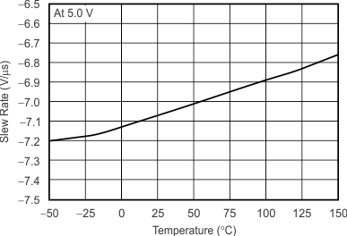
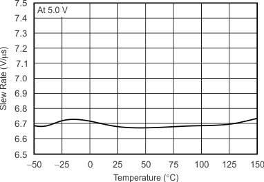
| SR | Slew rate(2) | RL = 10 kΩ to 2.5 V VREFIN = 2.5 V CMVR = −1 V to 4 V |
6.5 | V/µs | ||
| tS | Settling time, large-signal(2) | RL = 10 kΩ to 2.5 V VREFIN = 2.5 V dV ±2 V to 1%, no external filter |
0.9 | µs | ||
| Settling time(2) | RL = 10 kΩ to 2.5 V VREFIN = 2.5 V dV ±0.4 V to 0.01% |
14 | µs | |||
| INPUT RESISTANCE | ||||||
| Differential | RL = 10 kΩ to 2.5 V VREFIN = 2.5 V |
16.5 | 20 | 23.5 | kΩ | |
| Common-mode | RL = 10 kΩ to 2.5 V VREFIN = 2.5 V |
41 | 50 | 59 | kΩ | |
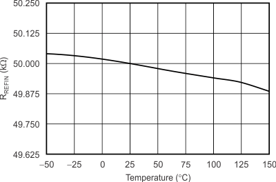
| External reference input | RL = 10 kΩ to 2.5 V VREFIN = 2.5 V |
41 | 50 | 59 | kΩ | |
| NOISE | ||||||
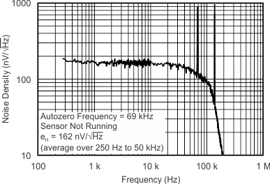
| en | Output voltage noise density, RTO(2) | RL = 10 kΩ to 2.5 V VREFIN = 2.5 V f = 1 kHz, compensation loop disabled |
170 | nV/√Hz | ||
| COMPENSATION LOOP | ||||||
| DC STABILITY | ||||||
| Offset error (3) | Probe f = 250 kHz, RLOAD = 20 Ω, deviation from 50% PWM, pin gain = L |
0.03% | ||||
| Offset error drift (2) | Probe f = 250 kHz, RLOAD = 20 Ω, deviation from 50% PWM, pin gain = L, TA = –40°C to 125°C |
7.5 | ppm/°C | |||
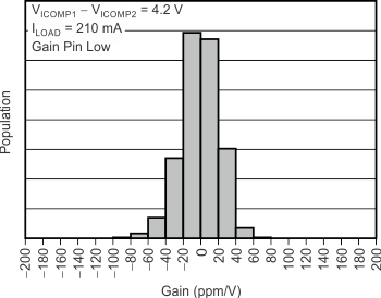
| Gain (2) | Probe f = 250 kHz, RLOAD = 20 Ω, pin gain = L, |VICOMP1| – |VICOMP2| |
–200 | 25 | 200 | ppm/V | |
| PSRR | Power-supply rejection ratio | Probe f = 250 kHz, RLOAD = 20 Ω | 500 | ppm/V | ||
| FREQUENCY RESPONSE | ||||||
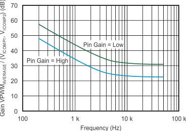
| Open-loop gain | Probe f = 250 kHz, RLOAD = 20 Ω, two modes, 7.8 kHz | 24/32 | dB | |||
| PROBE COIL LOOP | ||||||
| Input voltage clamp range | Field probe current < 50 mA | –0.7 to VDD + 0.7 | V | |||
| RHIGH | Internal resistor, IS1 or IS2 to VDD1 (2) | 47 | 59 | 71 | Ω | |
| RLOW | Internal resistor, IS1 or IS2 to GND1 (2) | 60 | 75 | 90 | Ω | |
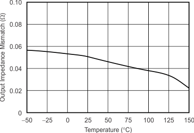
| Resistance mismatch between IS1 and IS2 (2) | ppm of RHIGH + RLOW | 300 | 1500 | ppm | ||
| Total input resistance | TA = –40°C to 125°C ICOMP = 0 mA |
134 | 200 | Ω | ||
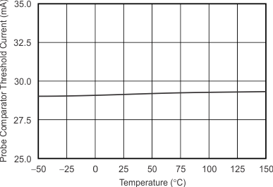
| Comparator threshold current | 22 | 28 | 34 | mA | ||
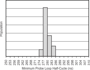
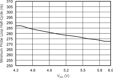
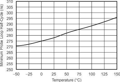
| Minimum probe loop half-cycle (2) | 250 | 280 | 310 | ns | ||
| Probe loop minimum frequency | 250 | kHz | ||||
| No oscillation detect (error) suppression | 35 | µs | ||||
| COMPENSATION COIL DRIVER, H-BRIDGE | ||||||
| Peak current (2) | VICOMP1 − VICOMP2 = 4 VPP
TA = –40°C to 125°C ICOMP = 0 mA |
250 | mA | |||
| Voltage swing | 20-Ω load | 4.2 | VPP | |||
| VOCM | Output common-mode voltage | VDD2 / 2 | V | |||
| Wire break detect, threshold current (4) | 33 | 57 | mA | |||
| VOLTAGE REFERENCE | ||||||
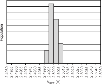
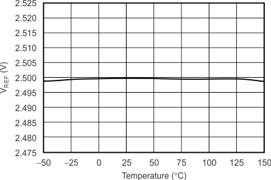
| Voltage (2) | No load | 2.495 | 2.5 | 2.505 | V | |
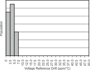
| Voltage drift (2) | No load, TA = – 40°C to 125°C ICOMP = 0 mA |
±5 | ±50 | ppm/°C | ||
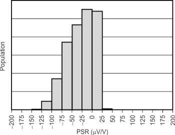
| PSRR | Power-supply rejection ratio(2) | ±15 | ±200 | µV/V | ||
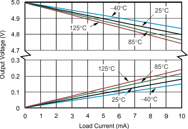
| Load regulation(2) | Load to GND and VDD
dI = 0 mA to 5 mA |
0.15 | mV/mA | |||
| ISC | Short-circuit current | REFOUT connected to VDD | 20 | mA | ||
| REFOUT connected to GND | –18 | mA | ||||
| DEMAGNETIZATION | ||||||
| Duration | At TA = –40°C to 125°C ICOMP = 0 mA; see the Demagnetization section |
106 | 130 | ms | ||
| DIGITAL I/O | ||||||
| LOGIC INPUTS (DEMAG, GAIN, and CCdiag PINS) | ||||||
| Pull-up high current (CCdiag) | CMOS-type levels, 3.5 < VIN < VDD | 160 | µA | |||
| Pull-up low current (CCdiag) | CMOS-type levels, 0 < VIN < 1.5 | 5 | µA | |||
| Logic input leakage current | CMOS-type levels, 0 < VIN < VDD | 0.01 | µA | |||
| Logic level, input: L/H | CMOS-type levels | 2.1/2.8 | ||||
| Hysteresis | CMOS-type levels | 0.7 | ||||
| OUTPUTS (ERROR AND OVER-RANGE PINS) | ||||||
| Logic level, output: L | 4-mA sink | 0.3 | V | |||
| Logic level, input: H | No internal pull-up | |||||
| OUTPUTS (PWM AND PWM PINS) | ||||||
| Logic level L | Push-pull type, 4-mA sink | 0.2 | V | |||
| Logic level H | Push-pull type, 4-mA source | VDD – 0.4 | V | |||
| POWER SUPPLY | ||||||
| VDD | Specified voltage range | TA = –40°C to 125°C ICOMP = 0 mA |
4.5 | 5 | 5.5 | V |
| VRST | Power-on reset threshold | 1.8 | V | |||
| IQ | Quiescent current [I(VDD1) + I(VDD2)] | ICOMP = 0 mA, sensor not connected | 6.8 | mA | ||
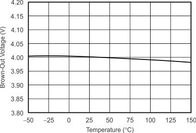
| Brownout voltage level | 4 | V | ||||
| Brownout indication delay | 135 | µs | ||||
| TEMPERATURE RANGE | ||||||
| TJ | Specified range | –40 | 125 | °C | ||
| TJ | Operating range | –50 | 150 | °C | ||
(1) Parameter value referred-to-output (RTO).
(2) See the Typical Characteristics curves.
(3) For VAC sensors, 0.2% of PWM offset approximately corresponds to 10-mA primary current per offset per winding.
6.6 Typical Characteristics
at TA = 25°C and VDD1 = VDD2 = 5 V with external 100-kHz filter bandwidth, (unless otherwise noted)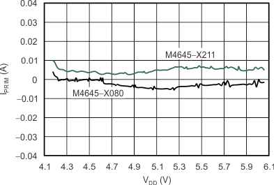
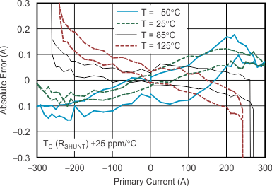
| Measurements by Vacuumschmelze GmbH. | ||
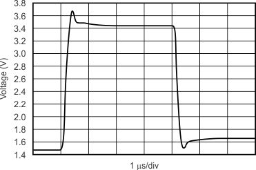
| TA = −50°C |
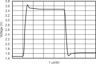
| TA = 150°C | ||
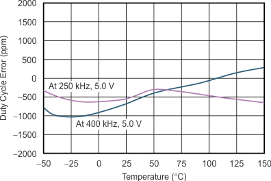
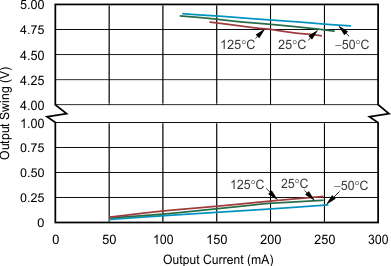
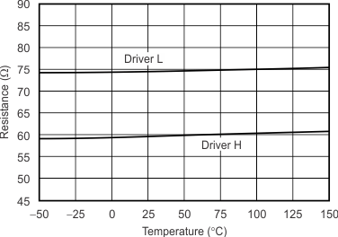
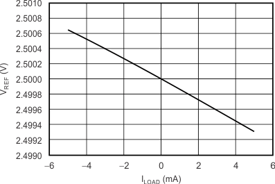
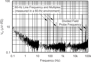
| Sensor M4645−X080, RSHUNT = 10 Ω, Mode = Low | ||
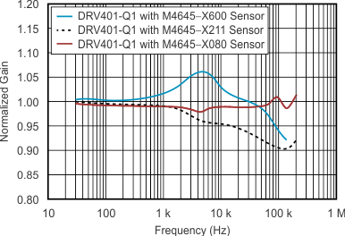
| Soldered DWP−20 with 1-in2 copper pad. Measurements by Vacuumschmelze GmbH. |
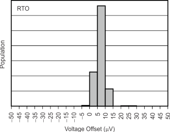
| Measurements by Vacuumschmelze GmbH. | ||
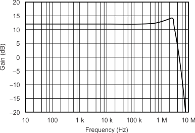
| TA = 25°C |
