SBOS988A August 2019 – April 2020 DRV425-Q1
PRODUCTION DATA.
- 1 Features
- 2 Applications
- 3 Description
- 4 Revision History
- 5 Pin Configuration and Functions
- 6 Specifications
- 7 Detailed Description
- 8 Application and Implementation
- 9 Power Supply Recommendations
- 10Layout
- 11Device and Documentation Support
- 12Mechanical, Packaging, and Orderable Information
Package Options
Mechanical Data (Package|Pins)
- RTJ|20
Thermal pad, mechanical data (Package|Pins)
Orderable Information
8.2.2.2 Detailed Design Procedure
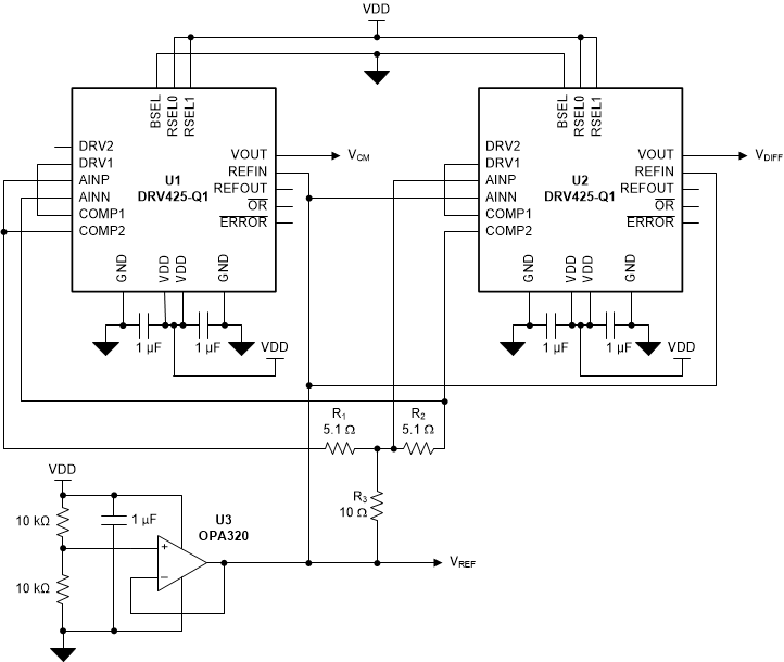
Figure 73 shows the schematic diagram of a differential gradient field measurement circuit.
 Figure 73. Busbar Current-Sensing Circuit
 In Figure 73, the feedback loops of both DRV425-Q1 sensors are combined to directly produce differential output VDIFF that is proportional to the sensed magnetic field difference inside the busbar hole. Both compensation coils are connected in series and are driven from a single side of the compensation coil driver (the DRV1 pins of each DRV425-Q1). Therefore, both driver stages make sure that a current proportional to the magnetic fields BR and BL is driven through the respective compensation coil. The difference in current through both compensation coils, and thus the difference field between the sensors, flows through resistor R3, and is sensed by the shunt-sense amplifier of U2. The current proportional to the common-mode field inside the busbar hole flows through R1 and R2, and is sensed by the shunt-sense amplifier of U1.
Use the output VCM to verify that the sensors are correctly positioned in the busbar hole with the following steps:
- Measure VCM with no current flow through the busbar and the PCB in the middle of the busbar hole. This value is the offset voltage VOFFSET. The value of VOFFSET only depends on stray fields and varies little with the absolute position of the sensors.
- Apply current through the busbar and move the PCB along the y-axis in the busbar hole, as shown in Figure 72. The PCB is in the center of the hole if VCM = VOFFSET.
The sensitivity drift performance of the circuit shown in Figure 73 is dominated by the temperature coefficient of the external resistors R1, R2, and R3. Select low-drift resistors for best sensor performance. For overall system error calculation, also consider the affect of thermal expansion on the PCB and busbar.
The internal voltage reference of the DRV425-Q1 cannot be used in this application because of its limited driver capability. The OPA320 (U3) is a low-noise operational amplifier with a short-circuit current capability of ±65 mA, and is used to support the required compensation current.
The advantage of this solution is the simplicity: the currents are subtracted by the two DRV425-Q1 devices without additional components. The series connection of the compensation coils halves the voltage swing, and reduces the measurement range of the sensors also by 50%. If a larger sensing range is required, operate the two sensors independently, and use a differential amplifier or ADC to subtract both voltage outputs (VOUT).
Use the ERROR outputs for fast overcurrent detection on the system level.