SLIS162I December   2014  – February 2023 DRV5013-Q1

PRODUCTION DATA  

  1. Features
  2. Applications
  3. Description
  4. Revision History
  5. Pin Configuration and Functions
  6. Specifications
    1. 6.1 Absolute Maximum Ratings
    2. 6.2 ESD Ratings
    3. 6.3 Recommended Operating Conditions
    4. 6.4 Thermal Information
    5. 6.5 Electrical Characteristics
    6. 6.6 Switching Characteristics
    7. 6.7 Magnetic Characteristics
    8. 6.8 Typical Characteristics
  7. Detailed Description
    1. 7.1 Overview
    2. 7.2 Functional Block Diagram
    3. 7.3 Feature Description
      1. 7.3.1 Field Direction Definition
      2. 7.3.2 Device Output
      3. 7.3.3 Power-On Time
      4. 7.3.4 Output Stage
      5. 7.3.5 Protection Circuits
        1. 7.3.5.1 Overcurrent Protection (OCP)
        2. 7.3.5.2 Load Dump Protection
        3. 7.3.5.3 Reverse Supply Protection
    4. 7.4 Device Functional Modes
  8. Application and Implementation
    1. 8.1 Application Information
    2. 8.2 Typical Applications
      1. 8.2.1 Standard Circuit
        1. 8.2.1.1 Design Requirements
        2. 8.2.1.2 Detailed Design Procedure
          1. 8.2.1.2.1 Configuration Example
        3. 8.2.1.3 Application Curves
      2. 8.2.2 Alternative Two-Wire Application
        1. 8.2.2.1 Design Requirements
        2. 8.2.2.2 Detailed Design Procedure
    3. 8.3 Power Supply Recommendations
    4. 8.4 Layout
      1. 8.4.1 Layout Guidelines
      2. 8.4.2 Layout Example
  9. Device and Documentation Support
    1. 9.1 Device Support
      1. 9.1.1 Device Nomenclature
      2. 9.1.2 Device Markings
    2. 9.2 Receiving Notification of Documentation Updates
    3. 9.3 Support Resources
    4. 9.4 Trademarks
    5. 9.5 Electrostatic Discharge Caution
    6. 9.6 Glossary
  10. 10Mechanical, Packaging, and Orderable Information

Package Options

Mechanical Data (Package|Pins)
Thermal pad, mechanical data (Package|Pins)
Orderable Information

Description

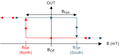
The DRV5013-Q1 device is a chopper-stabilized Hall effect sensor that offers a magnetic sensing solution with superior sensitivity stability over temperature and integrated protection features.

The magnetic field is indicated through a digital bipolar latch output. The IC has an open-drain output stage with 30-mA current sink capability. A wide operating voltage range from 2.7 V to 38 V with reverse polarity protection up to –22 V makes the device suitable for a wide range of automotive applications.

Internal protection functions are provided for reverse supply conditions, load dump, and output short circuit or overcurrent.

Package Information(1)
PART NUMBER PACKAGE BODY SIZE (NOM)
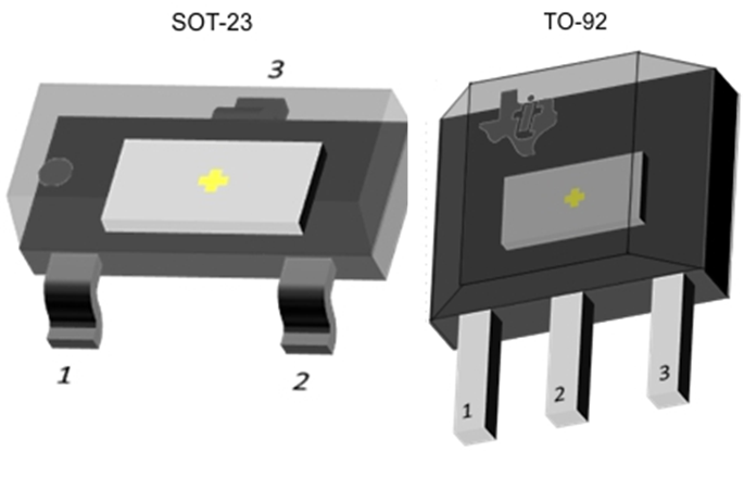
DRV5013-Q1 SOT-23 (3) 2.92 mm × 1.30 mm
TO-92 (3) 4.00 mm × 3.15 mm
For all available packages, see the package option addendum at the end of the data sheet.
GUID-AD162B48-81DC-471F-AA88-9F1608229FCF-low.gifOutput State
GUID-615A9CA8-E80B-45E3-949A-BE0B43611A3E-low.pngDevice Packages