SBAS915A June   2018  – April 2019 DRV5015

PRODUCTION DATA.  

  1. Features
  2. Applications
  3. Description
    1.     Device Images
      1.      Typical Schematic
      2.      Magnetic Response
  4. Revision History
  5. Pin Configuration and Functions
    1.     Pin Functions
  6. Specifications
    1. 6.1 Absolute Maximum Ratings
    2. 6.2 ESD Ratings
    3. 6.3 Recommended Operating Conditions
    4. 6.4 Thermal Information
    5. 6.5 Electrical Characteristics
    6. 6.6 Magnetic Characteristics
    7. 6.7 Typical Characteristics
  7. Detailed Description
    1. 7.1 Overview
    2. 7.2 Functional Block Diagram
    3. 7.3 Feature Description
      1. 7.3.1 Magnetic Flux Direction
      2. 7.3.2 Magnetic Response
      3. 7.3.3 Output Driver
      4. 7.3.4 Power-On Time
      5. 7.3.5 Hall Element Location
      6. 7.3.6 Propagation Delay
    4. 7.4 Device Functional Modes
  8. Application and Implementation
    1. 8.1 Application Information
    2. 8.2 Typical Applications
      1. 8.2.1 BLDC Motor Sensors Application
        1. 8.2.1.1 Design Requirements
        2. 8.2.1.2 Detailed Design Procedure
        3. 8.2.1.3 Application Curve
      2. 8.2.2 Incremental Rotary Encoding Application
        1. 8.2.2.1 Design Requirements
        2. 8.2.2.2 Detailed Design Procedure
        3. 8.2.2.3 Application Curve
    3. 8.3 What to Do and What Not to Do
  9. Power Supply Recommendations
  10. 10Layout
    1. 10.1 Layout Guidelines
    2. 10.2 Layout Example
  11. 11Device and Documentation Support
    1. 11.1 Documentation Support
      1. 11.1.1 Related Documentation
    2. 11.2 Receiving Notification of Documentation Updates
    3. 11.3 Community Resources
    4. 11.4 Trademarks
    5. 11.5 Electrostatic Discharge Caution
    6. 11.6 Glossary
  12. 12Mechanical, Packaging, and Orderable Information

Package Options

Mechanical Data (Package|Pins)
Thermal pad, mechanical data (Package|Pins)
Orderable Information

Output Driver

Figure 14 shows the DRV5015 open-drain output structure. An open-drain output offers flexibility by enabling system designers to interface to wide-range GPIO termination voltages. C1 represents the input capacitance of the GPIO. R1 represents the pullup resistor connected to the termination voltage, VPULL-UP. The maximum allowable value of VPULL_UP is 5.5 V. The value of R1 must be selected after proper considerations among the system speed and the power dissipation through the pullup resistor.
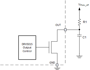
DRV5015 drv5015-open-drain.gifFigure 14. Open-Drain Output (Simplified)