SLIS163G December 2014 – March 2017 DRV5023-Q1
PRODUCTION DATA.
- 1 Features
- 2 Applications
- 3 Description
- 4 Revision History
- 5 Pin Configuration and Functions
- 6 Specifications
- 7 Detailed Description
- 8 Application and Implementation
- 9 Power Supply Recommendations
- 10Layout
- 11Device and Documentation Support
- 12Mechanical, Packaging, and Orderable Information
Package Options
Mechanical Data (Package|Pins)
Thermal pad, mechanical data (Package|Pins)
Orderable Information
8 Application and Implementation
NOTE
Information in the following applications sections is not part of the TI component specification, and TI does not warrant its accuracy or completeness. TI’s customers are responsible for determining suitability of components for their purposes. Customers should validate and test their design implementation to confirm system functionality.
8.1 Application Information
The DRV5023-Q1 device is used in magnetic-field sensing applications.
8.2 Typical Applications
8.2.1 Standard Circuit
 Figure 20. Typical Application Circuit
8.2.1.1 Design Requirements
For this design example, use the parameters listed in Table 2 as the input parameters.
Table 2. Design Parameters
| DESIGN PARAMETER | REFERENCE | EXAMPLE VALUE |
|---|---|---|
| Supply voltage | VCC | 3.2 to 3.4 V |
| System bandwidth | ƒBW | 10 kHz |
8.2.1.2 Detailed Design Procedure
Table 3. External Components
| COMPONENT | PIN 1 | PIN 2 | RECOMMENDED |
|---|---|---|---|
| C1 | VCC | GND | A 0.01-µF (minimum) ceramic capacitor rated for VCC |
| C2 | OUT | GND | Optional: Place a ceramic capacitor to GND |
| R1 | OUT | REF(1) | Requires a resistor pullup |
8.2.1.2.1 Configuration Example
In a 3.3-V system, 3.2 V ≤ Vref ≤ 3.4 V. Use Equation 3 to calculate the allowable range for R1.

For this design example, use Equation 4 to calculate the allowable range of R1.

Therefore:
After finding the allowable range of R1 (Equation 5), select a value between 500 Ω and 32 kΩ for R1.
Assuming a system bandwidth of 10 kHz, use Equation 6 to calculate the value of C2.

For this design example, use Equation 7 to calculate the value of C2.

An R1 value of 10 kΩ and a C2 value less than 820 pF satisfy the requirement for a 10-kHz system bandwidth.
A selection of R1 = 10 kΩ and C2 = 680 pF would cause a low-pass filter with a corner frequency of 23.4 kHz.
8.2.1.3 Application Curves

| R1 = 10-kΩ pullup | No C2 |

| R1 = 10-kΩ pullup | C2 = 680 pF |

| R1 = 10-kΩ pullup | C2 = 680 pF |
8.2.2 Alternative Two-Wire Application
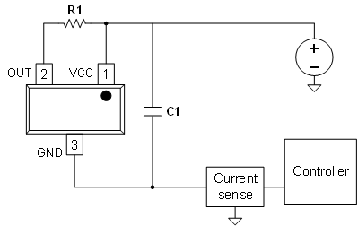
For systems that require minimal wire count, the device output can be connected to VCC through a resistor, and the total supplied current can be sensed near the controller.
 Figure 24. 2-Wire Application
Current can be sensed using a shunt resistor or other circuitry.
8.2.2.1 Design Requirements
Table 4 lists the related design parameters.
Table 4. Design Parameters
| DESIGN PARAMETER | REFERENCE | EXAMPLE VALUE |
|---|---|---|
| Supply voltage | VCC | 12 V |
| OUT resistor | R1 | 1 kΩ |
| Bypass capacitor | C1 | 0.1 µF |
| Current when B < BRP | IRELEASE | About 3 mA |
| Current when B > BOP | IOPERATE | About 15 mA |
8.2.2.2 Detailed Design Procedure
When the open-drain output of the device is high-impedance, current through the path equals the ICC of the device (approximately 3 mA).
When the output pulls low, a parallel current path is added, equal to VCC / (R1 + rDS(on)). Using 12 V and 1 kΩ, the parallel current is approximately 12 mA, making the total current approximately 15 mA.
The local bypass capacitor C1 should be at least 0.1 µF, and a larger value if there is high inductance in the power line interconnect.