SLVSDC7G April 2017 – July 2024 DRV5032
PRODUCTION DATA
- 1
- 1 Features
- 2 Applications
- 3 Description
- 4 Device Comparison
- 5 Pin Configuration and Functions
- 6 Specifications
- 7 Detailed Description
- 8 Application and Implementation
- 9 Device and Documentation Support
- 10Revision History
- 11Mechanical, Packaging, and Orderable Information
Package Options
Refer to the PDF data sheet for device specific package drawings
Mechanical Data (Package|Pins)
- DBZ|3
- DMR|4
- LPG|3
Thermal pad, mechanical data (Package|Pins)
- DMR|4
Orderable Information
5 Pin Configuration and Functions
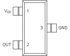 Figure 5-1 FA, FB,
FC, AJ, ZE Versions DBZ Package3-Pin
SOT-23Top View
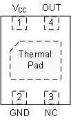 Figure 5-3 FA, AJ Versions
DMR Package4-Pin X2SONTop View
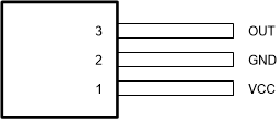 Figure 5-5 FA, FB, FC, AJ, ZE Versions LPG Package3-Pin TO-92Top View
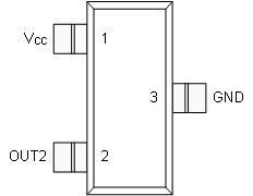 Figure 5-2 DU
Version DBZ Package3-Pin SOT-23Top View
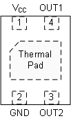 Figure 5-4 DU, DG, FD Versions DMR Package4-Pin X2SONTop View
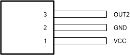 Figure 5-6 DU, FD Versions LPG Package3-Pin TO-92Top View
Table 5-1 Pin Functions
| PIN | I/O | DESCRIPTION | |||||||
|---|---|---|---|---|---|---|---|---|---|
| NAME | SOT-23 (FA, FB, FC, AJ, ZE) | SOT-23 (DU) | TO-92 (FA, FB, FC, AJ, ZE) | TO-92 (DU, FD) | X2SON (FA, AJ) | X2SON (DU, DG, FD) | |||
| GND | 3 | 3 | 2 | 2 | 2 | 2 | — | Ground reference | |
| OUT | 2 | — | 3 | — | 4 | — | O | Omnipolar output that responds to north and south magnetic poles | |
| OUT1 | — | — | — | — | — | 4 | O | Unipolar output that responds to north magnetic poles near the top of the package | |
| OUT2 | — | 2 | — | 3 | — | 3 | O | Unipolar output that responds to south magnetic poles near the top of the package | |
| NC | — | — | — | — | 3 | — | — | No-connect. This pin is not connected to the silicon. Leave this pin floating or tied to ground. Solder the pin to the board for mechanical support. | |
| VCC | 1 | 1 | 1 | 1 | 1 | 1 | — | 1.65-V to 5.5-V power supply. TI recommends connecting this pin to a ceramic capacitor to ground with a value of at least 0.1 µF. | |
| Thermal Pad | — | — | — | — | PAD | PAD | — | No-connect. Leave this pin floating or tied to ground. Solder the pin to the board for mechanical support. | |