SLIS154A December 2014 – December 2015 DRV5053-Q1
PRODUCTION DATA.
- 1 Features
- 2 Applications
- 3 Description
- 4 Revision History
- 5 Pin Configuration and Functions
- 6 Specifications
- 7 Detailed Description
- 8 Application and Implementation
- 9 Power Supply Recommendations
- 10Device and Documentation Support
- 11Mechanical, Packaging, and Orderable Information
Package Options
Mechanical Data (Package|Pins)
Thermal pad, mechanical data (Package|Pins)
Orderable Information
8 Application and Implementation
NOTE
Information in the following applications sections is not part of the TI component specification, and TI does not warrant its accuracy or completeness. TI’s customers are responsible for determining suitability of components for their purposes. Customers should validate and test their design implementation to confirm system functionality.
8.1 Application Information
The DRV5053-Q1 device is used in magnetic-field sensing applications.
8.2 Typical Applications
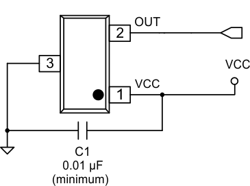
8.2.1 Typical Application With No Filter
 Figure 12. Typical Application Schematic – No Filter
8.2.1.1 Design Requirements
For this design example, use the parameters listed in Table 2 as the input parameters.
Table 2. Design Parameters
| DESIGN PARAMETER | REFERENCE | EXAMPLE VALUE |
|---|---|---|
| System bandwidth | ƒBW | 15 kHz |
8.2.1.2 Detailed Design Procedure
The DRV5053-Q1 has internal filtering that limits the bandwidth to at least 20 kHz. For this application no external components are required other than the C1 bypass capacitor, which is 0.01 µF minimum. If the analog output OUT is tied to a microcontroller ADC input, the equivalent load must be R > 10 kΩ and C < 10 nF.
Table 3. External Components
| COMPONENT | PIN 1 | PIN 2 | RECOMMENDED |
|---|---|---|---|
| C1 | VCC | GND | A 0.01-µF (minimum) ceramic capacitor rated for VCC |
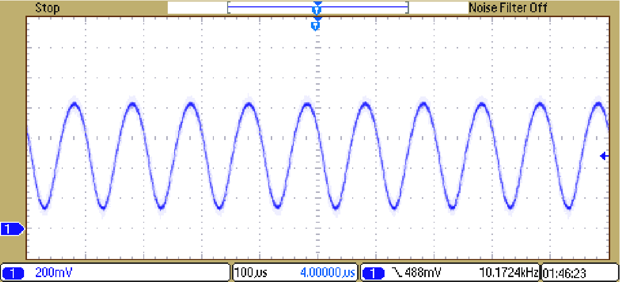
8.2.1.3 Application Curve

8.2.2 Filtered Typical Application
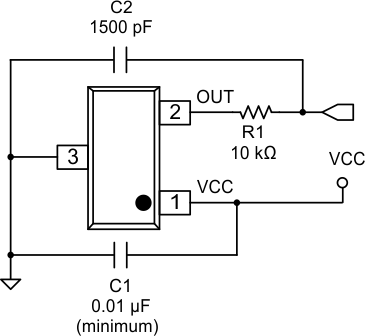
For lower noise on the analog output OUT, additional RC filtering can be added to further reduce the bandwidth.
 Figure 14. Filtered Typical Application Schematic
8.2.2.1 Design Requirements
For this design example, use the parameters listed in Table 4 as the input parameters.
Table 4. Design Parameters
| DESIGN PARAMETER | REFERENCE | EXAMPLE VALUE |
|---|---|---|
| System bandwidth | ƒBW | 5 kHz |
8.2.2.2 Detailed Design Procedure
In this example we will add an external RC filter in order to reduce the output bandwidth.
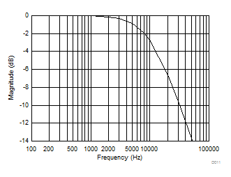
In order to preserve the signal at the frequencies of interest, we will conservatively select a low-pass filter bandwidth (–3-dB point) at twice the system bandwidth (10 kHz).

If we guess R1 = 10 kΩ, then C2 < 1590 pF. So we select C2 = 1500 pF.
8.2.2.2.1 Typical Noise Versus Cutoff Frequency
RC filters are an effective way to reduce the noise present on OUT. The following shows typical noise measurements for different cutoff frequencies using the DRV5053VA.
Table 5. DRV5053VA Typical Noise Data
| R (Ω) | C (µF) | fCUTOFF (kHz) | NOISE (mVpp) |
|---|---|---|---|
| 163 | 0.1 | 9.8 | 30.4 |
| 349 | 0.1 | 4.6 | 22.8 |
| 750 | 0.1 | 2.1 | 15.2 |
| 1505 | 0.1 | 1.1 | 9.7 |
| 3322 | 0.1 | 0.5 | 5.3 |
| 7510 | 0.1 | 0.2 | 2.5 |
8.2.2.3 Application Curves


| R1 = 10-kΩ pullup | C2 = 680 pF |