SLVSH22 May 2024 DRV8000-Q1
ADVANCE INFORMATION
- 1
- 1 Features
- 2 Applications
- 3 Description
- 4 Device Comparison
- 5 Pin Configuration and Functions
- 6 Specifications
-
7 Detailed Description
- 7.1 Overview
- 7.2 Functional Block Diagram
- 7.3 External Components
- 7.4
Feature Description
- 7.4.1 Heater MOSFET Driver
- 7.4.2 High-side Drivers
- 7.4.3 Electro-chromic Glass Driver
- 7.4.4 Half-bridge Drivers
- 7.4.5
Gate Drivers
- 7.4.5.1 Input PWM Modes
- 7.4.5.2
Smart Gate Driver - Functional Block
Diagram
- 7.4.5.2.1 Smart Gate Driver
- 7.4.5.2.2 Functional Block Diagram
- 7.4.5.2.3 Slew Rate Control (IDRIVE)
- 7.4.5.2.4 Gate Driver State Machine (TDRIVE)
- 7.4.5.2.5 Propagation Delay Reduction (PDR)
- 7.4.5.2.6 PDR Pre-Charge/Pre-Discharge Control Loop Operation Details
- 7.4.5.2.7 PDR Post-Charge/Post-Discharge Control Loop Operation Details
- 7.4.5.2.8 Detecting Drive and Freewheel MOSFET
- 7.4.5.2.9 Automatic Duty Cycle Compensation (DCC)
- 7.4.5.2.10 Closed Loop Slew Time Control (STC)
- 7.4.5.3 Tripler (Double-Stage) Charge Pump
- 7.4.5.4 Wide Common Mode Differential Current Shunt Amplifier
- 7.4.5.5 Gate Driver Protection Circuits
- 7.4.6 Sense Output (IPROPI)
- 7.4.7
Protection Circuits
- 7.4.7.1 Fault Reset (CLR_FLT)
- 7.4.7.2 DVDD Logic Supply Power on Reset (DVDD_POR)
- 7.4.7.3 PVDD Supply Undervoltage Monitor (PVDD_UV)
- 7.4.7.4 PVDD Supply Overvoltage Monitor (PVDD_OV)
- 7.4.7.5 VCP Charge Pump Undervoltage Lockout (VCP_UV)
- 7.4.7.6 Thermal Clusters
- 7.4.7.7 Watchdog Timer
- 7.4.7.8 Fault Detection and Response Summary Table
- 7.5 Programming
- 8 DRV8000-Q1 Register Map
- 9 DRV8000-Q1_STATUS Registers
- 10DRV8000-Q1_CNFG Registers
- 11DRV8000-Q1_CTRL Registers
- 12Application and Implementation
- 13Device and Documentation Support
- 14Revision History
- 15Mechanical, Packaging, and Orderable Information
Package Options
Mechanical Data (Package|Pins)
- RGZ|48
Thermal pad, mechanical data (Package|Pins)
Orderable Information
7.4.5.4 Wide Common Mode Differential Current Shunt Amplifier
The device integrates a high-performance, wide common-mode, bidirectional, current-shunt amplifiers for current measurements using shunt resistors in the external half-bridges. Current measurements are commonly used to implement overcurrent protection, external torque control, or commutation with an external controller. Due to the high common-mode range of the shunt amplifier, it can support low-side, high-side, or inline shunt configurations. The current shunt amplifiers include features such as programmable gain, unidirectional and bidirectional support, output blanking, and a programmable internal voltage reference to set a mid point bias voltage for the amplifier output. A simplified block diagram is shown in Figure 7-30. SP should connect to the positive terminal of the shunt resistor and SN should connect to the negative terminal of the shunt resistor. If the amplifiers are not utilized, the SN, SP inputs can be tied to PCB GND and the SO output left floating.
 Figure 7-30 Amplifier Simplified Block Diagram
A detailed block diagram is shown in . The wide common mode amplifier is implemented with a two stage differential architecture. The 1st differential stage supports a wide common mode input, differential output, and has a fixed gain, G = 2. The 2nd differential stage supports a variable gain adjustment, G = 5, 10, 20, or 40. The total gain of the two stages will be G = 10, 20, 40, or 80.
The internal reference voltage goes to a divider network, a buffer, and then sets the output voltage bias for the differential amplifier. The gain is configured through the register setting CSA_GAIN and the reference division ratio through CSA_DIV.
 Figure 7-31 Amplifier Detailed Block Diagram
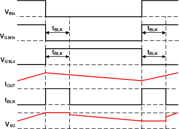
Lastly, the amplifier has an output blanking switch. The output switch can be used to disconnect the amplifier output during PWM switching to reduce output noise (blanking). The blanking circuit can be set to trigger on the active half-bridge through the CSA_BLK_SEL register setting. The blanking period can be configured through the CSA_BLK register setting. If the gate drivers are transitioning between high-side and low-side FET turn on and turn off or vice versa, the blanking time will extend through the dead-time window to avoid amplifier signal noise if the output swings or noise couples during the dead-time period. An output hold up capacitor is recommended to stabilize the amplifier output when it is disconnected during blanking. Typically this capacitor should be after a series resistor in a RC filter configuration to limit direct capacitance seen directly at the amplifier output. An example of the blanking function is shown in Figure 7-32.
 Figure 7-32 Amplifier Blanking
Example