SLVSH22 May 2024 DRV8000-Q1
ADVANCE INFORMATION
- 1
- 1 Features
- 2 Applications
- 3 Description
- 4 Device Comparison
- 5 Pin Configuration and Functions
- 6 Specifications
-
7 Detailed Description
- 7.1 Overview
- 7.2 Functional Block Diagram
- 7.3 External Components
- 7.4
Feature Description
- 7.4.1 Heater MOSFET Driver
- 7.4.2 High-side Drivers
- 7.4.3 Electro-chromic Glass Driver
- 7.4.4 Half-bridge Drivers
- 7.4.5
Gate Drivers
- 7.4.5.1 Input PWM Modes
- 7.4.5.2
Smart Gate Driver - Functional Block
Diagram
- 7.4.5.2.1 Smart Gate Driver
- 7.4.5.2.2 Functional Block Diagram
- 7.4.5.2.3 Slew Rate Control (IDRIVE)
- 7.4.5.2.4 Gate Driver State Machine (TDRIVE)
- 7.4.5.2.5 Propagation Delay Reduction (PDR)
- 7.4.5.2.6 PDR Pre-Charge/Pre-Discharge Control Loop Operation Details
- 7.4.5.2.7 PDR Post-Charge/Post-Discharge Control Loop Operation Details
- 7.4.5.2.8 Detecting Drive and Freewheel MOSFET
- 7.4.5.2.9 Automatic Duty Cycle Compensation (DCC)
- 7.4.5.2.10 Closed Loop Slew Time Control (STC)
- 7.4.5.3 Tripler (Double-Stage) Charge Pump
- 7.4.5.4 Wide Common Mode Differential Current Shunt Amplifier
- 7.4.5.5 Gate Driver Protection Circuits
- 7.4.6 Sense Output (IPROPI)
- 7.4.7
Protection Circuits
- 7.4.7.1 Fault Reset (CLR_FLT)
- 7.4.7.2 DVDD Logic Supply Power on Reset (DVDD_POR)
- 7.4.7.3 PVDD Supply Undervoltage Monitor (PVDD_UV)
- 7.4.7.4 PVDD Supply Overvoltage Monitor (PVDD_OV)
- 7.4.7.5 VCP Charge Pump Undervoltage Lockout (VCP_UV)
- 7.4.7.6 Thermal Clusters
- 7.4.7.7 Watchdog Timer
- 7.4.7.8 Fault Detection and Response Summary Table
- 7.5 Programming
- 8 DRV8000-Q1 Register Map
- 9 DRV8000-Q1_STATUS Registers
- 10DRV8000-Q1_CNFG Registers
- 11DRV8000-Q1_CTRL Registers
- 12Application and Implementation
- 13Device and Documentation Support
- 14Revision History
- 15Mechanical, Packaging, and Orderable Information
Package Options
Mechanical Data (Package|Pins)
- RGZ|48
Thermal pad, mechanical data (Package|Pins)
Orderable Information
7.4.5.2.4 Gate Driver State Machine (TDRIVE)
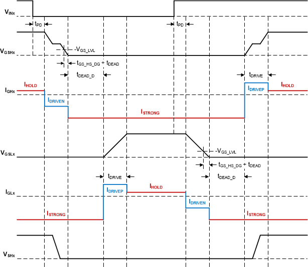
The TDRIVE component of the smart gate drive architecture is an integrated gate drive state machine that provides automatic dead time insertion, parasitic dV/dt gate coupling prevention, and MOSFET gate fault detection.
The first component of the TDRIVE state machine is an automatic dead time handshake. Dead time is the period of body diode conduction time between the switching of the external high-side and low-side MOSFET to prevent any cross conduction or shoot through. The gate drivers of DRV8000-Q1 use VGS monitors to implement a break and then make dead time scheme by measuring the external MOSFET VGS voltage to determine when to properly enable the external MOSFETs. This scheme allows the gate driver to adjust the dead time for variations in the system such as temperature drift, aging, voltage fluctuations, and variation in the external MOSFET parameters. An additional fixed digital dead time (tDEAD_D) can be inserted if desired and is adjustable through the SPI registers.
The second component focuses on preventing parasitic dV/dt gate charge coupling. This is implemented by enabling a strong gate current pull-down (ISTRONG) whenever the opposite MOSFET in the half-bridge is switching. This feature helps remove parasitic charge that couples into the external MOSFET gate when the half-bridge switch node is rapidly slewing.
The third component implements a gate fault detection scheme to detect an issue with the gate voltage. This is used to detect pin-to-pin solder defects, a MOSFET gate failure, or a gate stuck high or stuck low voltage condition. This is done by using the VGS monitors to measure the gate voltage after the end of the tDRIVE time. If the gate voltage has not reached the proper threshold, the gate driver will report the corresponding fault condition. To ensure a false fault is not detected, a tDRIVE time should be selected that is longer than the time required to charge or discharge the MOSFET gate. The tDRIVE time does not impact the PWM minimum duration and will terminate early if another PWM command is received.
 Figure 7-25 TDRIVE
Turn On / Off