SLLSFA9B July 2020 – June 2021 DRV8106-Q1
PRODUCTION DATA
- 1 Features
- 2 Applications
- 3 Descriptions
- 4 Revision History
- 5 Pin Configuration
- 6 Specifications
-
7 Detailed Description
- 7.1 Overview
- 7.2 Functional Block Diagram
- 7.3
Feature Description
- 7.3.1 External Components
- 7.3.2 Device Interface Variants
- 7.3.3 Input PWM Modes
- 7.3.4 Smart Gate Driver
- 7.3.5 Doubler (Single-Stage) Charge Pump
- 7.3.6 Wide Common Mode Differential Current Shunt Amplifier
- 7.3.7 Pin Diagrams
- 7.3.8
Protection and Diagnostics
- 7.3.8.1 Gate Driver Disable and Enable (DRVOFF and EN_DRV)
- 7.3.8.2 Fault Reset (CLR_FLT)
- 7.3.8.3 DVDD Logic Supply Power on Reset (DVDD_POR)
- 7.3.8.4 PVDD Supply Undervoltage Monitor (PVDD_UV)
- 7.3.8.5 PVDD Supply Overvoltage Monitor (PVDD_OV)
- 7.3.8.6 VCP Charge Pump Undervoltage Lockout (VCP_UV)
- 7.3.8.7 MOSFET VDS Overcurrent Protection (VDS_OCP)
- 7.3.8.8 Gate Driver Fault (VGS_GDF)
- 7.3.8.9 Thermal Warning (OTW)
- 7.3.8.10 Thermal Shutdown (OTSD)
- 7.3.8.11 Offline Short Circuit and Open Load Detection (OOL and OSC)
- 7.3.8.12 Fault Detection and Response Summary Table
- 7.4 Device Function Modes
- 7.5 Programming
- 7.6 Register Maps
- 8 Application and Implementation
- 9 Power Supply Recommendations
- 10Layout
- 11Device and Documentation Support
- 12Mechanical, Packaging, and Orderable Information
Package Options
Refer to the PDF data sheet for device specific package drawings
Mechanical Data (Package|Pins)
- RHB|32
Thermal pad, mechanical data (Package|Pins)
- RHB|32
Orderable Information
3 Descriptions
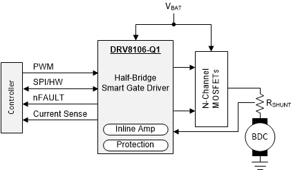
The DRV8106-Q1 is a highly integrated half-bridge gate driver, capable of driving high-side and low-side N-channel power MOSFETs. It generates the proper gate drive voltages using an integrated doubler charge pump for the high-side and a linear regulator for the low-side.
The device uses a smart gate drive architecture to reduce system cost and improve reliability. The gate driver optimizes dead time to avoid shoot-through conditions, provides control to decreasing electromagnetic interference (EMI) through adjustable gate drive current, and protects against drain to source and gate short conditions with VDS and VGS monitors.
A wide common mode shunt amplifier provides inline current sensing to continuously measure motor current even during recirculating windows. The amplifier can be used in low-side or high-side sense configurations if inline sensing is not required.
The DRV8106-Q1 provide an array of protection features to ensure robust system operation. These include under and overvoltage monitors for the power supply and charge pump, VDS overcurrent and VGS gate fault monitors for the external MOSFETs, offline open load and short circuit diagnostics, and internal thermal warning and shutdown protection.
| PART NUMBER | PACKAGE | BODY SIZE (NOM) |
|---|---|---|
| DRV8106-Q1 | VQFN (32) | 5.00 mm x 5.00 mm |
 Simplified Schematic