SLLSFA9B July 2020 – June 2021 DRV8106-Q1
PRODUCTION DATA
- 1 Features
- 2 Applications
- 3 Descriptions
- 4 Revision History
- 5 Pin Configuration
- 6 Specifications
-
7 Detailed Description
- 7.1 Overview
- 7.2 Functional Block Diagram
- 7.3
Feature Description
- 7.3.1 External Components
- 7.3.2 Device Interface Variants
- 7.3.3 Input PWM Modes
- 7.3.4 Smart Gate Driver
- 7.3.5 Doubler (Single-Stage) Charge Pump
- 7.3.6 Wide Common Mode Differential Current Shunt Amplifier
- 7.3.7 Pin Diagrams
- 7.3.8
Protection and Diagnostics
- 7.3.8.1 Gate Driver Disable and Enable (DRVOFF and EN_DRV)
- 7.3.8.2 Fault Reset (CLR_FLT)
- 7.3.8.3 DVDD Logic Supply Power on Reset (DVDD_POR)
- 7.3.8.4 PVDD Supply Undervoltage Monitor (PVDD_UV)
- 7.3.8.5 PVDD Supply Overvoltage Monitor (PVDD_OV)
- 7.3.8.6 VCP Charge Pump Undervoltage Lockout (VCP_UV)
- 7.3.8.7 MOSFET VDS Overcurrent Protection (VDS_OCP)
- 7.3.8.8 Gate Driver Fault (VGS_GDF)
- 7.3.8.9 Thermal Warning (OTW)
- 7.3.8.10 Thermal Shutdown (OTSD)
- 7.3.8.11 Offline Short Circuit and Open Load Detection (OOL and OSC)
- 7.3.8.12 Fault Detection and Response Summary Table
- 7.4 Device Function Modes
- 7.5 Programming
- 7.6 Register Maps
- 8 Application and Implementation
- 9 Power Supply Recommendations
- 10Layout
- 11Device and Documentation Support
- 12Mechanical, Packaging, and Orderable Information
Package Options
Refer to the PDF data sheet for device specific package drawings
Mechanical Data (Package|Pins)
- RHB|32
Thermal pad, mechanical data (Package|Pins)
- RHB|32
Orderable Information
9.1 Bulk Capacitance
Having appropriate local bulk capacitance is an important factor in motor drive system design. Having more bulk capacitance is generally beneficial, while the disadvantages are increased cost and physical size.
The amount of local bulk capacitance needed depends on a variety of factors, including:
- The highest current required by the motor or load
- The capacitance of the power supply and ability to source current
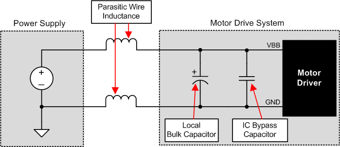
- The amount of parasitic inductance between the power supply and motor system
- The acceptable voltage ripple of the system
- The motor braking method (if applicable)
The inductance between the power supply and motor drive system limits how the rate current can change from the power supply. If the local bulk capacitance is too small, the system responds to excessive current demands or dumps from the motor with a change in voltage. When adequate bulk capacitance is used, the motor voltage remains stable and high current can be quickly supplied.
The data sheet generally provides a recommended minimum value, but system level testing is required to determine the appropriately sized bulk capacitor.
 Figure 9-1 System Supply Parasitics Example