SLLSFA9B July 2020 – June 2021 DRV8106-Q1
PRODUCTION DATA
- 1 Features
- 2 Applications
- 3 Descriptions
- 4 Revision History
- 5 Pin Configuration
- 6 Specifications
-
7 Detailed Description
- 7.1 Overview
- 7.2 Functional Block Diagram
- 7.3
Feature Description
- 7.3.1 External Components
- 7.3.2 Device Interface Variants
- 7.3.3 Input PWM Modes
- 7.3.4 Smart Gate Driver
- 7.3.5 Doubler (Single-Stage) Charge Pump
- 7.3.6 Wide Common Mode Differential Current Shunt Amplifier
- 7.3.7 Pin Diagrams
- 7.3.8
Protection and Diagnostics
- 7.3.8.1 Gate Driver Disable and Enable (DRVOFF and EN_DRV)
- 7.3.8.2 Fault Reset (CLR_FLT)
- 7.3.8.3 DVDD Logic Supply Power on Reset (DVDD_POR)
- 7.3.8.4 PVDD Supply Undervoltage Monitor (PVDD_UV)
- 7.3.8.5 PVDD Supply Overvoltage Monitor (PVDD_OV)
- 7.3.8.6 VCP Charge Pump Undervoltage Lockout (VCP_UV)
- 7.3.8.7 MOSFET VDS Overcurrent Protection (VDS_OCP)
- 7.3.8.8 Gate Driver Fault (VGS_GDF)
- 7.3.8.9 Thermal Warning (OTW)
- 7.3.8.10 Thermal Shutdown (OTSD)
- 7.3.8.11 Offline Short Circuit and Open Load Detection (OOL and OSC)
- 7.3.8.12 Fault Detection and Response Summary Table
- 7.4 Device Function Modes
- 7.5 Programming
- 7.6 Register Maps
- 8 Application and Implementation
- 9 Power Supply Recommendations
- 10Layout
- 11Device and Documentation Support
- 12Mechanical, Packaging, and Orderable Information
Package Options
Refer to the PDF data sheet for device specific package drawings
Mechanical Data (Package|Pins)
- RHB|32
Thermal pad, mechanical data (Package|Pins)
- RHB|32
Orderable Information
7.3.6 Wide Common Mode Differential Current Shunt Amplifier
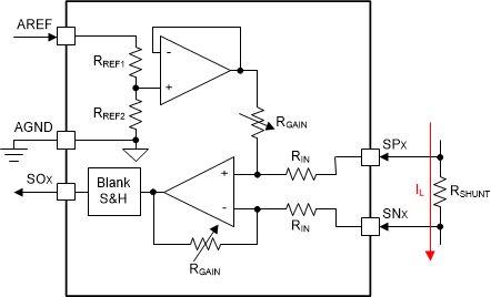
The DRV8106-Q1 integrates a high-performance, wide common-mode, bidirectional, current-shunt amplifier for current measurements using a shunt resistor in the external half-bridge. Current measurements are commonly used to implement overcurrent protection, external torque control, or commutation with an external controller. Due to the high common-mode range of the shunt amplifier it can support low-side, high-side, or inline shunt configurations. The current shunt amplifiers include features such as programmable gain, unidirectional and bidirectional support, output blanking and sample and hold switch, and a dedicated voltage reference pin (AREF) to set a mid point bias voltage for the amplifier output. A simplified block diagram is shown in Figure 7-7. SP should connect to the positive terminal of the shunt resistor and SN should connect to the negative terminal of the shunt resistor. If the amplifier is not utilized, the AREF, SN, SP inputs can be tied to AGND, AGND to PCB GND and the SO output left floating.
 Figure 7-7 Amplifier Simplified Block Diagram
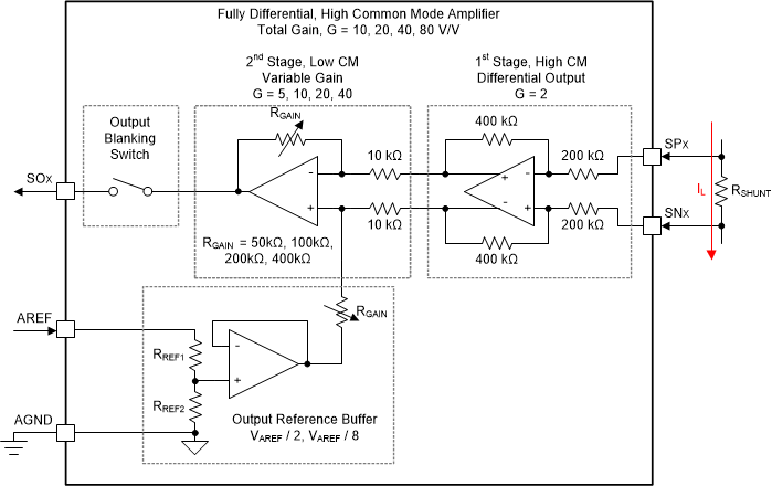
A detailed block diagram is shown in Figure 7-8. The wide common mode amplifier is implemented with a two stage differential architecture. The 1st differential stage supports a wide common mode input, differential output, and has a fixed gain, G = 2. The 2nd differential stage supports a variable gain adjustment, G = 5, 10, 20, or 40. The total gain of the two stages will be G = 10, 20, 40, or 80.
The amplifier can also generate an output voltage bias through the AREF pin. The AREF pin goes to a divider network, a buffer, and then sets the output voltage bias for the differential amplifier. On SPI device variants, the gain is configured through the register setting CSA_GAIN and the reference division ratio through CSA_DIV. On H/W device variants, the reference division ratio is fixed to VAREF / 2. The gain is configured through the GAIN pin.
 Figure 7-8 Amplifier Detailed Block Diagram
Lastly, the amplifier has an output blanking or sample and hold switch. This option is only available on SPI device variants. The output switch can be used to disconnect the amplifier output during PWM switching to reduce output noise (blanking) or during motor braking to maintain the output value if the shunt is used in high-side or low-side configuration (sample and hold). The blanking circuit can be set trigger on the active half-bridge (half-bridge 1 or half-bridge 2) through the CSA_BLK_SEL register setting. The blanking period can be configured through the CSA_BLK register setting. The sample and hold circuit can be enabled with the CSA_SH_EN register setting. When active, the sample and hold will trigger whenever the driver enters high-side or low-side braking. To utilize either the blanking or sample and hold functions and output hold up capacitor will be required to stabilize the amplifier output when it is disconnected. Typically it is recommended, that this capacitor be after a series resistor in a RC filter configuration to limit direct capacitance seen directly at the amplifier output.
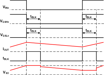
 Figure 7-9 DRV8106-Q1 Amplifier Blanking Example
Figure 7-9 shows an example of the amplifier blanking function. This function can be utilized to hi-Z the amplifier output during a switching transition, but is not required by default. This function can be beneficial if noise due to wide-common mode swings or ground shifts are occurring during the PWM switching transition and interfering with the amplifier output. As shown in the image, the blanking function operates by disabling the amplifier output for a period of time after a transition on either GHx or GLx. This period of time is determined by the tBLK setting configured through the CSA_BLK register setting.
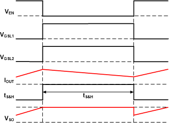
 Figure 7-10 DRV8106-Q1 Amplifier Sample & Hold Example
Figure 7-10 show an example of the amplifier sample and hold function. This function can be utilized to hi-Z the amplifier output when the current is recirculating in the H-bridge, but is not required by default. The function can be beneficial if the shunt resistor is configured into the low-side or the high-side of the H-bridge in which during current recirculation the current information is lost. As shown in the image, the sample and hold function will hold the previous state of the amplifier output since the output capacitor will remain charged. The amplifier will resume operation when the H-bridge leaves the recirculation state.