SLVSGC3 May   2020 DRV8210P

PRODUCTION DATA  

  1. Features
  2. Applications
  3. Description
  4. Revision History
  5. Device Comparison
  6. Pin Configuration and Functions
  7. Specifications
    1. 7.1 Absolute Maximum Ratings
    2. 7.2 ESD Ratings
    3. 7.3 Recommended Operating Conditions
    4. 7.4 Thermal Information
    5. 7.5 Electrical Characteristics
    6. 7.6 Typical Characteristics
  8. Detailed Description
    1. 8.1 Overview
    2. 8.2 Functional Block Diagram
    3. 8.3 Feature Description
      1. 8.3.1 External Components
      2. 8.3.2 Control Modes
        1. 8.3.2.1 PWM Control
      3. 8.3.3 Protection Circuits
        1. 8.3.3.1 Supply Undervoltage Lockout (UVLO)
        2. 8.3.3.2 OUTx Overcurrent Protection (OCP)
        3. 8.3.3.3 Thermal Shutdown (TSD)
      4. 8.3.4 Pin Diagrams
        1. 8.3.4.1 Logic-Level Inputs
    4. 8.4 Device Functional Modes
      1. 8.4.1 Active Mode
      2. 8.4.2 Low-Power Sleep Mode
      3. 8.4.3 Fault Mode
  9. Application and Implementation
    1. 9.1 Application Information
    2. 9.2 Typical Application
      1. 9.2.1 Full-Bridge Driving
        1. 9.2.1.1 Design Requirements
        2. 9.2.1.2 Detailed Design Procedure
          1. 9.2.1.2.1 Supply Voltage
          2. 9.2.1.2.2 Control Interface
          3. 9.2.1.2.3 Low-Power Operation
        3. 9.2.1.3 Application Curves
      2. 9.2.2 Dual-Coil Relay Driving
        1. 9.2.2.1 Design Requirements
        2. 9.2.2.2 Detailed Design Procedure
          1. 9.2.2.2.1 Supply Voltage
          2. 9.2.2.2.2 Control Interface
          3. 9.2.2.2.3 Low-Power Operation
        3. 9.2.2.3 Application Curves
      3. 9.2.3 Current Sense
        1. 9.2.3.1 Design Requirements
        2. 9.2.3.2 Detailed Design Procedure
          1. 9.2.3.2.1 Shunt Resistor Sizing
    3. 9.3 Current Capability and Thermal Performance
      1. 9.3.1 Power Dissipation and Output Current Capability
      2. 9.3.2 Thermal Performance
        1. 9.3.2.1 Steady-State Thermal Performance
        2. 9.3.2.2 Transient Thermal Performance
  10. 10Power Supply Recommendations
    1. 10.1 Bulk Capacitance
  11. 11Layout
    1. 11.1 Layout Guidelines
    2. 11.2 Layout Example
  12. 12Device and Documentation Support
    1. 12.1 Documentation Support
      1. 12.1.1 Related Documentation
    2. 12.2 Receiving Notification of Documentation Updates
    3. 12.3 Support Resources
    4. 12.4 Trademarks
    5. 12.5 Electrostatic Discharge Caution
    6. 12.6 Glossary
  13. 13Mechanical, Packaging, and Orderable Information

Package Options

Mechanical Data (Package|Pins)
Thermal pad, mechanical data (Package|Pins)
Orderable Information

Bulk Capacitance

Having appropriate local bulk capacitance is an important factor in motor drive system design. Having more bulk capacitance is generally beneficial, while the disadvantages are increased cost and physical size.

The amount of local bulk capacitance needed depends on a variety of factors, including:

  • The highest current required by the motor or load
  • The capacitance of the power supply and ability to source current
  • The amount of parasitic inductance between the power supply and motor system
  • The acceptable voltage ripple of the system
  • The motor braking method (if applicable)

The inductance between the power supply and motor drive system limits how the rate current can change from the power supply. If the local bulk capacitance is too small, the system responds to excessive current demands or dumps from the motor with a change in voltage. When adequate bulk capacitance is used, the motor voltage remains stable and high current can be quickly supplied.

The data sheet generally provides a recommended minimum value, but system level testing is required to determine the appropriately sized bulk capacitor.
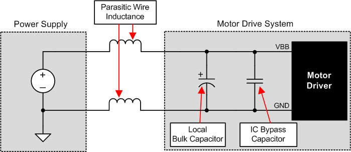
GUID-A1967E42-3D71-4D2A-9C57-60A2A08FBC93-low.gif Figure 10-1 System Supply Parasitics Example