SLVSGC3 May 2020 DRV8210P
PRODUCTION DATA
- 1 Features
- 2 Applications
- 3 Description
- 4 Revision History
- 5 Device Comparison
- 6 Pin Configuration and Functions
- 7 Specifications
- 8 Detailed Description
- 9 Application and Implementation
- 10Power Supply Recommendations
- 11Layout
- 12Device and Documentation Support
- 13Mechanical, Packaging, and Orderable Information
Package Options
Mechanical Data (Package|Pins)
- DSG|8
Thermal pad, mechanical data (Package|Pins)
- DSG|8
Orderable Information
9.3.2 Thermal Performance
The datasheet-specified junction-to-ambient thermal resistance, RθJA, is primarily useful for comparing various drivers or approximating thermal performance. However, the actual system performance may be better or worse than this value depending on PCB stackup, routing, number of vias, and copper area around the thermal pad. The length of time the driver drives a particular current will also impact power dissipation and thermal performance. This section considers how to design for steady-state and transient thermal conditions.
The data in this section was simulated using the following criteria:
- 2-layer PCB, standard FR4, 1-oz (35 mm copper thickness) or 2-oz copper
thickness. Thermal vias are only present under the thermal pad (2 vias, 1.2mm
spacing, 0.3 mm diameter, 0.025 mm Cu plating).
- Top layer: DRV8210P WSON package footprint and copper plane heatsink. Top layer copper area is varied in simulation.
- Bottom layer: ground plane thermally connected through vias under the thermal pad for DRV8210P. Bottom layer copper area varies with top copper area.
- 4-layer PCB, standard FR4. Outer planes are 1-oz (35 mm copper thickness) or
2-oz copper thickness. Inner planes are kept at 1-oz. Thermal vias are only
present under the thermal pad (2 vias, 1.2mm spacing, 0.3 mm diameter, 0.025 mm
Cu plating).
- Top layer: DRV8210P WSON package footprint and copper plane heatsink. Top layer copper area is varied in simulation.
- Mid layer 1: GND plane thermally connected to DRV8210P thermal pad through vias. The area of the ground plane is 74.2 mm x 74.2 mm.
- Mid layer 2: power plane, no thermal connection. The area of the power plane is 74.2 mm x 74.2 mm.
- Bottom layer: signal layer with small copper pad underneath DRV8210P and thermally connected through via stitching from the TOP and internal GND planes. Bottom layer thermal pad is the same size as the package (2 mm x 2 mm). Bottom pad size remains constant as top copper plane is varied.
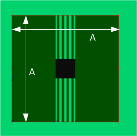
Figure 9-13 shows an example of the simulated board for the HTSSOP package. Table 9-5 shows the dimensions of the board that were varied for each simulation.
 Figure 9-13 WSON PCB model top
layer
Figure 9-13 WSON PCB model top
layer| Cu area (mm2) | Dimension A (mm) |
|---|---|
| 2 | 15.11 |
| 4 | 20.98 |
| 8 | 29.27 |
| 16 | 40.99 |