SLVSH04 November 2023 DRV8214
PRODUCTION DATA
- 1
- 1 Features
- 2 Applications
- 3 Description
- 4 Revision History
- 5 Device Comparison
- 6 Pin Configuration and Functions
- 7 Specifications
-
8 Detailed Description
- 8.1 Overview
- 8.2 Functional Block Diagram
- 8.3
Feature Description
- 8.3.1 External Components
- 8.3.2 Summary of Features
- 8.3.3 Bridge Control
- 8.3.4 Current Sense and Regulation (IPROPI)
- 8.3.5 Stall Detection
- 8.3.6
Ripple Counting
- 8.3.6.1
Ripple Counting Parameters
- 8.3.6.1.1 Motor Resistance Inverse
- 8.3.6.1.2 Motor Resistance Inverse Scale
- 8.3.6.1.3 KMC Scaling Factor
- 8.3.6.1.4 KMC
- 8.3.6.1.5 Filter Damping Constant
- 8.3.6.1.6 Filter Input Scaling Factor
- 8.3.6.1.7 Ripple Count Threshold
- 8.3.6.1.8 Ripple Count Threshold Scale
- 8.3.6.1.9 T_MECH_FLT
- 8.3.6.1.10 VSNS_SEL
- 8.3.6.1.11 Error Correction
- 8.3.6.2 RC_OUT Output
- 8.3.6.3 Ripple Counting with nFAULT
- 8.3.6.1
Ripple Counting Parameters
- 8.3.7 Motor Voltage and Speed Regulation
- 8.3.8 Protection Circuits
- 8.4 Device Functional Modes
- 8.5 Programming
- 8.6 Register Map
-
9 Application and Implementation
- 9.1 Application Information
- 9.2 Typical Application: Brushed DC Motor
- 10Power Supply Recommendations
- 11Layout
- 12Mechanical, Packaging, and Orderable Information
Package Options
Mechanical Data (Package|Pins)
- RTE|16
Thermal pad, mechanical data (Package|Pins)
- RTE|16
Orderable Information
9.2.6 Application Curves
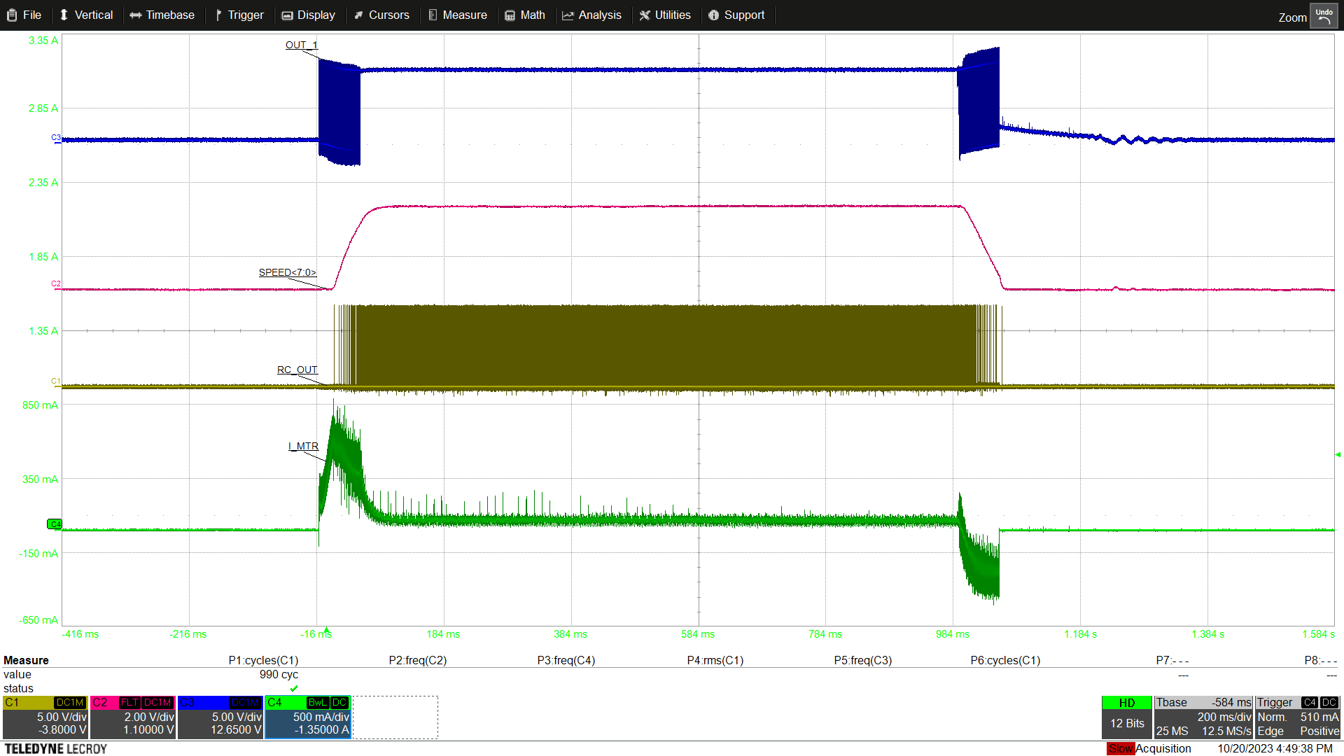
 Figure 9-5 Example Operation at VM = 5.00
V. RC_OUT denotes the pulse train output of the RC_OUT pin
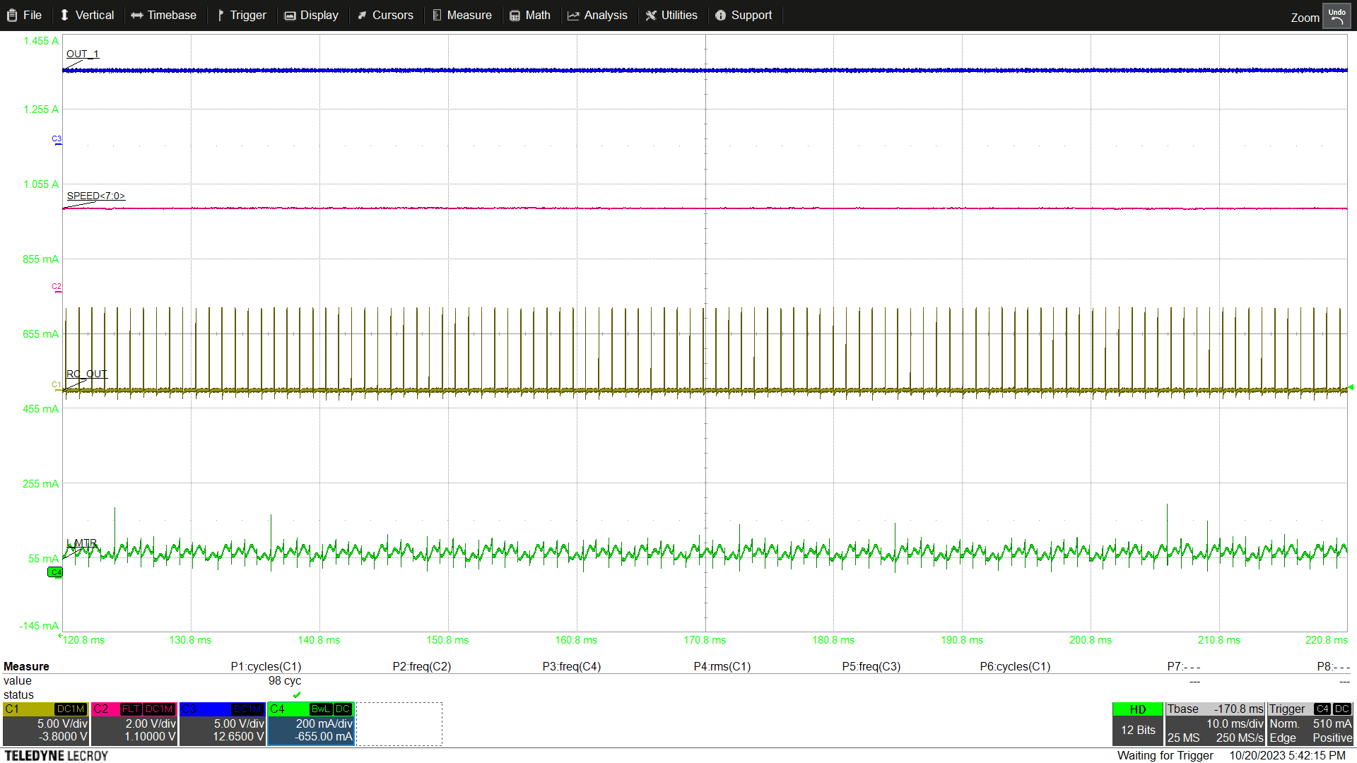
 Figure 9-6 Steady State Operation at VM = 5 V. RC_OUT denotes the pulse train output of the RC_OUT pin
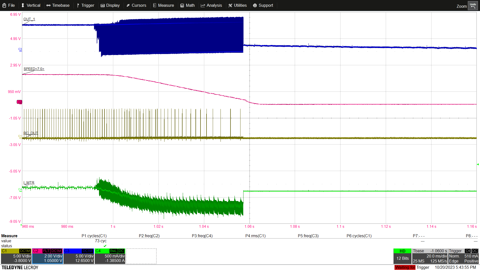
 Figure 9-7 Soft Stop at VM = 5 V. RC_OUT denotes the pulse train output of the RC_OUT pin
 Figure 9-8 Transient Loading Conditions -
Full Profile. RC_OUT denotes the pulse train output of the RC_OUT pin