SLVSFZ7 November   2021 DRV8231

PRODUCTION DATA  

  1. Features
  2. Applications
  3. Description
  4. Revision History
  5. Device Comparison
  6. Pin Configuration and Functions
  7. Specifications
    1. 7.1 Absolute Maximum Ratings
    2. 7.2 ESD Ratings
    3. 7.3 Recommended Operating Conditions
    4. 7.4 Thermal Information
    5. 7.5 Electrical Characteristics
    6. 7.6 Typical Characteristics
    7. 7.7 Timing Diagrams
  8. Detailed Description
    1. 8.1 Overview
    2. 8.2 Functional Block Diagram
    3. 8.3 External Components
    4. 8.4 Feature Description
      1. 8.4.1 Bridge Control
      2. 8.4.2 Current Regulation
      3. 8.4.3 Protection Circuits
        1. 8.4.3.1 Overcurrent Protection (OCP)
        2. 8.4.3.2 Thermal Shutdown (TSD)
        3. 8.4.3.3 VM Undervoltage Lockout (UVLO)
    5. 8.5 Device Functional Modes
      1. 8.5.1 Active Mode
      2. 8.5.2 Low-Power Sleep Mode
      3. 8.5.3 Fault Mode
    6. 8.6 Pin Diagrams
      1. 8.6.1 Logic-Level Inputs
  9. Application and Implementation
    1. 9.1 Application Information
    2. 9.2 Typical Application
      1. 9.2.1 Brush DC Motor
        1. 9.2.1.1 Design Requirements
        2. 9.2.1.2 Detailed Design Procedure
          1. 9.2.1.2.1 Motor Voltage
          2. 9.2.1.2.2 Motor Current
          3. 9.2.1.2.3 Sense Resistor
        3. 9.2.1.3 Application Curves
      2. 9.2.2 Stall Detection
        1. 9.2.2.1 Design Requirements
        2. 9.2.2.2 Detailed Design Procedure
          1. 9.2.2.2.1 Stall Detection Timing
          2. 9.2.2.2.2 Stall Threshold Selection
        3. 9.2.2.3 Application Curves
      3. 9.2.3 Relay Driving
        1. 9.2.3.1 Design Requirements
        2. 9.2.3.2 Detailed Design Procedure
          1. 9.2.3.2.1 Control Interface for Single-Coil Relays
          2. 9.2.3.2.2 Control Interface for Dual-Coil Relays
        3. 9.2.3.3 Application Curves
      4. 9.2.4 Multi-Sourcing with Standard Motor Driver Pinout
    3. 9.3 Current Capability and Thermal Performance
      1. 9.3.1 Power Dissipation and Output Current Capability
      2. 9.3.2 Thermal Performance
        1. 9.3.2.1 Steady-State Thermal Performance
        2. 9.3.2.2 Transient Thermal Performance
  10. 10Power Supply Recommendations
    1. 10.1 Bulk Capacitance
  11. 11Layout
    1. 11.1 Layout Guidelines
    2. 11.2 Layout Example
  12. 12Device and Documentation Support
    1. 12.1 Documentation Support
      1. 12.1.1 Related Documentation
    2. 12.2 Receiving Notification of Documentation Updates
    3. 12.3 Community Resources
    4. 12.4 Trademarks
  13. 13Mechanical, Packaging, and Orderable Information

Package Options

Mechanical Data (Package|Pins)
Thermal pad, mechanical data (Package|Pins)
Orderable Information

Overcurrent Protection (OCP)

An analog current limit circuit on each FET limits the current through the FET by limiting the gate drive internally. If this analog current limit persists for longer than the OCP deglitch time (tOCP), all FETs in the H-bridge will disable. The driver re-enables after the OCP retry period (tRETRY) has passed. If the fault condition is still present, the cycle repeats as shown in Figure 8-4.
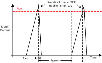
GUID-E423FF39-9403-4861-AD34-82C567D4B366-low.gif Figure 8-4 OCP Operation

Overcurrent conditions are detected independently on both high- and low-side FETs. This means that a short to ground, supply, or across the motor winding will all result in an overcurrent shutdown. The ISEN pin also integrates a separate overcurrent trip threshold specified by VOCP_ISEN for additional protection when the VM voltage is low or the RSENSE resistance on the ISEN pin is high.