SLVSH03 December   2023 DRV8234

PRODUCTION DATA  

  1.   1
  2. Features
  3. Applications
  4. Description
  5. Device Comparison
  6. Pin Configuration and Functions
  7. Specifications
    1. 6.1 Absolute Maximum Ratings
    2. 6.2 ESD Ratings
    3. 6.3 Recommended Operating Conditions
    4. 6.4 Thermal Information
    5. 6.5 Electrical Characteristics
    6. 6.6 I2C Timing Requirements
    7. 6.7 Timing Diagrams
    8. 6.8 Typical Operating Characteristics
  8. Detailed Description
    1. 7.1 Overview
    2. 7.2 Functional Block Diagram
    3. 7.3 Feature Description
      1. 7.3.1 External Components
      2. 7.3.2 Summary of Features
      3. 7.3.3 Bridge Control
      4. 7.3.4 Current Sense and Regulation (IPROPI)
        1. 7.3.4.1 Current Sensing
        2. 7.3.4.2 Current Regulation
          1. 7.3.4.2.1 Fixed Off-Time Current Regulation
          2. 7.3.4.2.2 Cycle-By-Cycle Current Regulation
      5. 7.3.5 Stall Detection
      6. 7.3.6 Ripple Counting
        1. 7.3.6.1 Ripple Counting Parameters
          1. 7.3.6.1.1  Motor Resistance Inverse
          2. 7.3.6.1.2  Motor Resistance Inverse Scale
          3. 7.3.6.1.3  KMC Scaling Factor
          4. 7.3.6.1.4  KMC
          5. 7.3.6.1.5  Filter Damping Constant
          6. 7.3.6.1.6  Filter Input Scaling Factor
          7. 7.3.6.1.7  Ripple Count Threshold
          8. 7.3.6.1.8  Ripple Count Threshold Scale
          9. 7.3.6.1.9  T_MECH_FLT
          10. 7.3.6.1.10 VSNS_SEL
          11. 7.3.6.1.11 Error Correction
            1. 7.3.6.1.11.1 EC_FALSE_PER
            2. 7.3.6.1.11.2 EC_MISS_PER
        2. 7.3.6.2 RC_OUT Output
        3. 7.3.6.3 Ripple Counting with nFAULT
      7. 7.3.7 Motor Voltage and Speed Regulation
        1. 7.3.7.1 Internal Bridge Control
        2. 7.3.7.2 Setting Speed/Voltage Regulation Parameters
          1. 7.3.7.2.1 Speed and Voltage Set
          2. 7.3.7.2.2 Speed Scaling Factor
        3. 7.3.7.3 Soft-Start and Soft-Stop
          1. 7.3.7.3.1 TINRUSH
      8. 7.3.8 Protection Circuits
        1. 7.3.8.1 Overcurrent Protection (OCP)
        2. 7.3.8.2 Thermal Shutdown (TSD)
        3. 7.3.8.3 VM Undervoltage Lockout (VM UVLO)
        4. 7.3.8.4 Overvoltage Protection (OVP)
        5. 7.3.8.5 nFAULT Output
    4. 7.4 Device Functional Modes
      1. 7.4.1 Active Mode
      2. 7.4.2 Low-Power Sleep Mode
      3. 7.4.3 Fault Mode
    5. 7.5 Programming
      1. 7.5.1 I2C Communication
        1. 7.5.1.1 I2C Write
        2. 7.5.1.2 I2C Read
    6. 7.6 Register Map
      1. 7.6.1 DRV8234_STATUS Registers
      2. 7.6.2 DRV8234_CONFIG Registers
      3. 7.6.3 DRV8234_CTRL Registers
  9. Application and Implementation
    1. 8.1 Application Information
    2. 8.2 Typical Application: Brushed DC Motor
      1. 8.2.1 Design Requirements
      2. 8.2.2 Stall Detection
        1. 8.2.2.1 Application Description
          1. 8.2.2.1.1 Stall Detection Timing
          2. 8.2.2.1.2 Hardware Stall Threshold Selection
      3. 8.2.3 Ripple Counting Application
        1. 8.2.3.1 Tuning Ripple Counting Parameters
          1. 8.2.3.1.1 Resistance Parameters
          2. 8.2.3.1.2 KMC and KMC_SCALE
            1. 8.2.3.1.2.1 Case I
            2. 8.2.3.1.2.2 Case II
              1. 8.2.3.1.2.2.1 Method 1: Tuning from Scratch
                1. 8.2.3.1.2.2.1.1 Tuning KMC_SCALE
                2. 8.2.3.1.2.2.1.2 Tuning KMC
              2. 8.2.3.1.2.2.2 Method 2: Using the Proportionality factor
                1. 8.2.3.1.2.2.2.1 Working Example
          3. 8.2.3.1.3 Advanced Parameters
            1. 8.2.3.1.3.1 Filter Constants
              1. 8.2.3.1.3.1.1 FLT_GAIN_SEL
              2. 8.2.3.1.3.1.2 FLT_K
            2. 8.2.3.1.3.2 T_MECH_FLT
            3. 8.2.3.1.3.3 VSNS_SEL
            4. 8.2.3.1.3.4 Additional Error Corrector Parameters
              1. 8.2.3.1.3.4.1 EC_FALSE_PER
              2. 8.2.3.1.3.4.2 EC_MISS_PER
      4. 8.2.4 Motor Voltage
      5. 8.2.5 Motor Current
      6. 8.2.6 Application Curves
  10. Power Supply Recommendations
    1. 9.1 Bulk Capacitance
  11. 10Layout
    1. 10.1 Layout Guidelines
  12. 11Device and Documentation Support
    1. 11.1 Receiving Notification of Documentation Updates
    2. 11.2 Support Resources
    3. 11.3 Trademarks
    4. 11.4 Electrostatic Discharge Caution
    5. 11.5 Glossary
  13. 12Revision History

Package Options

Mechanical Data (Package|Pins)
Thermal pad, mechanical data (Package|Pins)
Orderable Information

Overcurrent Protection (OCP)

An analog current limit circuit on each FET limits the current through the FET by limiting the gate drive internally. If this analog current limit persists for longer than the OCP deglitch time (tOCP), all FETs in the H-bridge will disable, FAULT and OCP bits become 1b and nFAULT is pulled low.

The OCP_MODE bit programs the response of the device to overcurrent event. The device can either latch-off or perform automatic retry to recover from an overcurrent event.

In automatic retry mode, the MOSFETs will be disabled and the nFAULT pin driven low for a duration of tRETRY. After tRETRY, the MOSFETs are re-enabled according to the control inputs. If the overcurrent condition is still present, the cycle repeats; otherwise normal device operation resumes. This is explained by the following diagram -
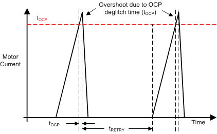
GUID-DA7A44B7-FCB2-46CF-A7FE-2BEA308C9942-low.gifFigure 7-17 OCP Operation

In latch-off mode, the MOSFETs will remain disabled and the nFAULT pin will be driven low until the device is reset by a CLR_FLT command or by cycling the VM power supply.

Overcurrent conditions are detected independently on both high- and low-side FETs. This means that a short to ground, supply, or across the motor winding will all result in an overcurrent shutdown. Overcurrent protection does not use the current sense circuitry used for current regulation, so it functions regardless of VREF and IPROPI settings.