SLVSHO3 April 2024 DRV8235
PRODUCTION DATA
- 1
- 1 Features
- 2 Applications
- 3 Description
- 4 Device Comparison
- 5 Pin Configuration and Functions
- 6 Specifications
-
7 Detailed Description
- 7.1 Overview
- 7.2 Functional Block Diagram
- 7.3
Feature Description
- 7.3.1 External Components
- 7.3.2 Summary of Features
- 7.3.3 Bridge Control
- 7.3.4 Current Sense and Regulation (IPROPI)
- 7.3.5 Stall Detection
- 7.3.6 Motor Voltage and Speed Regulation
- 7.3.7 Protection Circuits
- 7.4 Device Functional Modes
- 7.5 Programming
- 8 Register Map
- 9 Application and Implementation
- 10Device and Documentation Support
- 11Revision History
- 12Mechanical, Packaging, and Orderable Information
Package Options
Mechanical Data (Package|Pins)
- RTE|16
Thermal pad, mechanical data (Package|Pins)
- RTE|16
Orderable Information
7.3.4.2.2 Cycle-By-Cycle Current Regulation
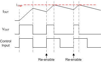
In cycle-by-cycle mode, the H-bridge enters a brake, low-side slow decay state (both low-side MOSFETs ON) after IOUT exceeds ITRIP until the next control input edge on either the EN/IN1 or PH/IN2 pins or 0 to 1 transitions on the I2C_EN_IN1 or I2C_PH_IN2 bits. This allows for additional control of the current regulation by the external controller. This is shown in the diagram below. Cycle-by-cycle mode will not support 100% duty cycle current regulation as a new control input edge is required to reset the outputs after the brake, low-side slow decay state has been entered.
 Figure 7-6 Cycle-By-Cycle Current Regulation
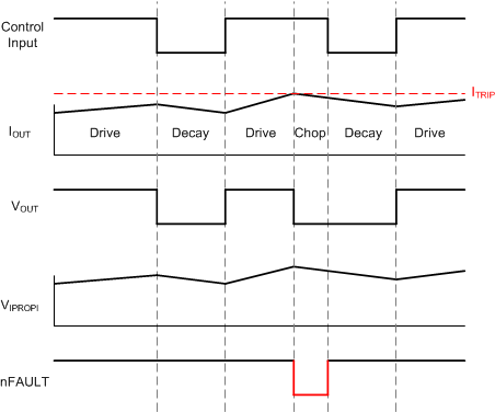
In cycle-by-cycle mode, the device can indicate whenever the H-bridge enters internal current regulation by pulling the nFAULT pin low. This can be used to determine when the device outputs will differ from the control inputs or the load has reached the ITRIP threshold. This behavior is controlled by the CBC_REP bit. This is shown in the following diagram. In cycle-by-cycle mode, if the CBC_REP bit is 1b, nFAULT will be pulled low when the H-bridge enters internal current regulation and nFAULT will be released whenever the next control input edge is received by the device and the outputs are reset.
 Figure 7-7 Cycle-By-Cycle Current Regulation, CBC_REP = 1b
No device functionality is affected when the nFAULT pin is pulled low for the current regulation indicator. The nFAULT pin is only used as an indicator and the device will continue normal operation. To distinguish a device fault from the current regulation indicator, the nFAULT pin can be compared with the control inputs. The current regulation indicator can only assert when the control inputs are commanding a forward or reverse drive state. If the nFAULT pin is pulled low and the control inputs are commanding the high-Z or slow-decay states, then a device fault has occurred.