SLVSG24C November 2021 – November 2022 DRV8244-Q1
PRODMIX
- 1 Features
- 2 Applications
- 3 Description
- 4 Revision History
- 5 Device Comparison
- 6 Pin Configuration and Functions
-
7 Specifications
- 7.1 Absolute Maximum Ratings
- 7.2 ESD Ratings
- 7.3 Recommended Operating Conditions
- 7.4 Thermal Information
- 7.5
Electrical Characteristics
- 7.5.1 Power Supply & Initialization
- 7.5.2 Logic I/Os
- 7.5.3 SPI I/Os
- 7.5.4 Configuration Pins - HW Variant Only
- 7.5.5 Power FET Parameters
- 7.5.6 Switching Parameters with High-Side Recirculation
- 7.5.7 Switching Parameters with Low-Side Recirculation
- 7.5.8 IPROPI & ITRIP Regulation
- 7.5.9 Over Current Protection (OCP)
- 7.5.10 Over Temperature Protection (TSD)
- 7.5.11 Voltage Monitoring
- 7.5.12 Load Monitoring
- 7.5.13 Fault Retry Setting
- 7.5.14 Transient Thermal Impedance & Current Capability
- 7.6 SPI Timing Requirements
- 7.7 Switching Waveforms
- 7.8 Typical Characteristics
- 8 Detailed Description
- 9 Application and Implementation
- 10Power Supply Recommendations
- 11Layout
- 12Device and Documentation Support
- 13Mechanical, Packaging, and Orderable Information
Package Options
Mechanical Data (Package|Pins)
Thermal pad, mechanical data (Package|Pins)
- DGQ|28
Orderable Information
10.1 Bulk Capacitance Sizing
Bulk capacitance sizing is an important factor in motor drive system design. It is beneficial to have more bulk capacitance, while the disadvantages are increased cost and physical size.
The amount of local capacitance needed depends on a variety of factors including:
- The highest current required by the motor system.
- The capacitance of the power supply and the ability of the power supply to source current.
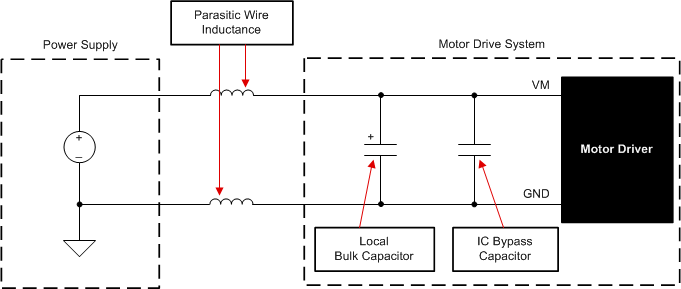
- The amount of parasitic inductance between the power supply and motor system.
- The acceptable voltage ripple.
- The type of motor used (brushed DC, brushless DC, and stepper).
- The motor braking method.
The inductance between the power supply and motor drive system limits the rate that current can change from the power supply. If the local bulk capacitance is too small, the system responds to excessive current demands or dumps from the motor with a change in voltage. When sufficient bulk capacitance is used, the motor voltage remains stable, and high current can be quickly supplied.
The data sheet provides a recommended value, but system-level testing is required to determine the appropriate sized bulk capacitor.
 Figure 10-1 Example Setup of Motor Drive System With External Power Supply
The voltage rating for bulk capacitors should be higher than the operating voltage to provide a margin for cases when the motor transfers energy to the supply.