SLVSG24C November 2021 – November 2022 DRV8244-Q1
PRODMIX
- 1 Features
- 2 Applications
- 3 Description
- 4 Revision History
- 5 Device Comparison
- 6 Pin Configuration and Functions
-
7 Specifications
- 7.1 Absolute Maximum Ratings
- 7.2 ESD Ratings
- 7.3 Recommended Operating Conditions
- 7.4 Thermal Information
- 7.5
Electrical Characteristics
- 7.5.1 Power Supply & Initialization
- 7.5.2 Logic I/Os
- 7.5.3 SPI I/Os
- 7.5.4 Configuration Pins - HW Variant Only
- 7.5.5 Power FET Parameters
- 7.5.6 Switching Parameters with High-Side Recirculation
- 7.5.7 Switching Parameters with Low-Side Recirculation
- 7.5.8 IPROPI & ITRIP Regulation
- 7.5.9 Over Current Protection (OCP)
- 7.5.10 Over Temperature Protection (TSD)
- 7.5.11 Voltage Monitoring
- 7.5.12 Load Monitoring
- 7.5.13 Fault Retry Setting
- 7.5.14 Transient Thermal Impedance & Current Capability
- 7.6 SPI Timing Requirements
- 7.7 Switching Waveforms
- 7.8 Typical Characteristics
- 8 Detailed Description
- 9 Application and Implementation
- 10Power Supply Recommendations
- 11Layout
- 12Device and Documentation Support
- 13Mechanical, Packaging, and Orderable Information
Package Options
Mechanical Data (Package|Pins)
Thermal pad, mechanical data (Package|Pins)
- DGQ|28
Orderable Information
11.2 Layout Example
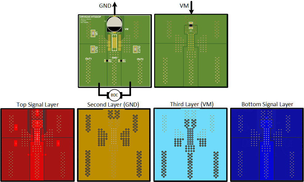
The following figure shows a layout example for a 4 cm X 4 cm x 1.6 mm, 4 layer PCB for a leaded package device. The 4 layers uses 2 oz copper on top/ bottom signal layers and 1 oz copper on internal supply layers, with 0.3 mm thermal via drill diameter, 0.025 mm Cu plating, 1 mm minimum via pitch. The same layout can be adopted for the non-leaded VQFN-HR package as well. The Section 7.5.14 for the 4 cm X 4 cm X 1.6 mm is based on a similar layout.
Note: The layout example shown is for a full bridge topology using DRV824xQ1 device in SSOP package.
 Figure 11-1 Layout example:
4cm x 4 cm x 1.6mm, 4 layer PCB