-
DRV8256E/P H-Bridge Motor Driver With Integrated Current Sense and Smart Tune Technology
- 1 Features
- 2 Applications
- 3 Description
- 4 Revision History
- 5 Pin Configuration and Functions
- 6 Specifications
- 7 Detailed Description
- 8 Application and Implementation
- 9 Power Supply Recommendations
- 10Layout
- 11Device and Documentation Support
- 12Mechanical, Packaging, and Orderable Information
- IMPORTANT NOTICE
Package Options
Mechanical Data (Package|Pins)
Thermal pad, mechanical data (Package|Pins)
- RGE|24
Orderable Information
DRV8256E/P H-Bridge Motor Driver With Integrated Current Sense and Smart Tune Technology
1 Features
- N-channel H-bridge motor driver
- Drives one bidirectional brushed-DC motor
- Two unidirectional brushed DC motors
- Integrated current sensing and regulation
- 4.5 V to 48 V Operating supply voltage range
- Multiple control interface options
- PHASE/ENABLE (PH/EN)
- PWM (IN/IN)
- Smart tune, fast and mixed decay options
- Low RDS(ON): 165 mΩ HS + LS at 24 V, 25°C
- High Output Current Capability: 6.4-A peak
- Limits inrush current of brushed-DC motors
- Configurable Off-Time PWM Chopping
- 7, 16, 24 or 32 μs
- Supports 1.8 V, 3.3 V, 5.0 V logic inputs
- Low-current sleep mode (2 µA)
- Spread spectrum clocking for low EMI
- Protection features
- VM undervoltage lockout (UVLO)
- Charge pump undervoltage (CPUV)
- Overcurrent protection (OCP)
- Thermal shutdown (OTSD)
- Fault condition output (nFAULT)
2 Applications
3 Description
The DRV8256E/P devices are single H-bridge motor drivers for a wide variety of industrial applications. The devices integrate an N-channel H-bridge, charge pump regulator, current sensing and regulation, and protection circuitry.
Integrated current sensing allows the driver to regulate the motor inrush current during start up and high load events. A current limit can be set with an adjustable external voltage reference. The integrated current sensing uses an internal current mirror architecture, removing the need for a large power shunt resistor, saving board area and reducing system cost. A low-power sleep mode is provided to achieve ultra-low quiescent current draw by shutting down most of the internal circuitry.
Internal protection features are provided for supply undervoltage lockout (UVLO), charge pump undervoltage (CPUV), output overcurrent (OCP), and device overtemperature (TSD). Fault conditions are indicated on nFAULT.
| PART NUMBER (1) | PACKAGE | BODY SIZE (NOM) |
|---|---|---|
| DRV8256EPWPR | HTSSOP (28) | 9.7mm x 4.4mm |
| DRV8256ERGER | VQFN (24) | 4.0mm x 4.0mm |
| DRV8256PPWPR | HTSSOP (28) | 9.7mm x 4.4mm |
| DRV8256PRGER | VQFN (24) | 4.0mm x 4.0mm |
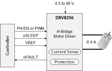 DRV8256 Simplified Schematic
5 Pin Configuration and Functions
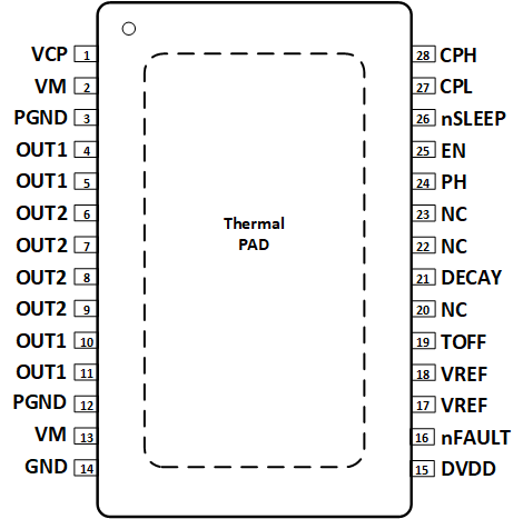 Figure 5-1 PWP PowerPAD™ Package28-Pin HTSSOPTop View DRV8256E
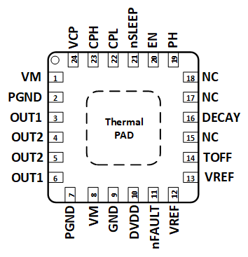 Figure 5-2 RGE Package24-Pin VQFN with Exposed Thermal PADTop View DRV8256E
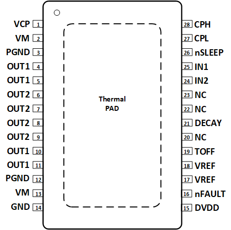 Figure 5-3 PWP PowerPAD™ Package28-Pin HTSSOPTop View DRV8256P
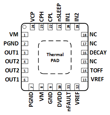 Figure 5-4 RGE Package24-Pin VQFN with Exposed Thermal PADTop View DRV8256P
Pin Functions
| PIN | TYPE | DESCRIPTION | ||||
|---|---|---|---|---|---|---|
| NAME | PWP | RGE | ||||
| DRV8256E | DRV8256P | DRV8256E | DRV8256P | |||
| DECAY | 21 | 21 | 16 | 16 | I | Decay mode setting pin. Quad-level pin. |
| EN | 25 | — | 20 | — | I | Enable input. Logic high enables bridge; logic low disables the bridge Hi-Z. |
| IN1 | — | 25 | — | 20 | I | PWM input. Logic controls the state of H-bridge; internal pulldown. |
| IN2 | — | 24 | — | 19 | I | PWM input. Logic controls the state of H-bridge; internal pulldown. |
| OUT1 | 4, 5, 10, 11 | 4, 5, 10, 11 | 3, 6 | 3, 6 | O | Winding output. Connect to motor winding. |
| OUT2 | 6, 7, 8, 9 | 6, 7, 8, 9 | 4, 5 | 4, 5 | O | Winding output. Connect to motor winding. |
| PH | 24 | — | 19 | — | I | Phase input. Logic high drives current from OUT1 to OUT2. |
| VREF | 17, 18 | 17, 18 | 12, 13 | 12, 13 | I | Reference voltage input pins. Voltage on these pins sets the full scale chopping current in H-bridge. The two pins must be tied together. |
| NC | 20, 22, 23 | 20, 22, 23 | 15, 17, 18 | 15, 17, 18 | I | No Connect. |
| CPH | 28 | 28 | 23 | 23 | PWR | Charge pump switching node. Connect a X7R, 0.022-μF, VM-rated ceramic capacitor from CPH to CPL. |
| CPL | 27 | 27 | 22 | 22 | ||
| GND | 14 | 14 | 9 | 9 | PWR | Device ground. Connect to system ground. |
| TOFF | 19 | 19 | 14 | 14 | I | Sets the decay mode off-time during current chopping; quad-level pin. Also sets the ripple current in smart tune ripple control mode. |
| DVDD | 15 | 15 | 10 | 10 | PWR | Logic supply voltage. Connect a X7R, 0.47-μF to 1-μF, 6.3-V or 10-V rated ceramic capacitor to GND. |
| VCP | 1 | 1 | 24 | 24 | O | Charge pump output. Connect a X7R, 0.22-μF, 16-V ceramic capacitor to VM. |
| VM | 2, 13 | 2, 13 | 1, 8 | 1, 8 | PWR | Power supply. Connect to motor supply voltage and bypass to PGND with two 0.01-μF ceramic capacitors (one for each pin) plus a bulk capacitor rated for VM. |
| PGND | 3, 12 | 3, 12 | 2, 7 | 2, 7 | PWR | Power ground. Connect to system ground. |
| nFAULT | 16 | 16 | 11 | 11 | O | Fault indication. Pulled logic low with fault condition; open-drain output requires an external pullup resistor. |
| nSLEEP | 26 | 26 | 21 | 21 | I | Sleep mode input. Logic high to enable device; logic low to enter low-power sleep mode; internal pulldown resistor. |
| PAD | - | - | - | - | - | Thermal pad. Connect to system ground. |