SLOSE50A April   2020  – June 2021

PRODUCTION DATA  

  1. Features
  2. Applications
  3. Description
  4. Revision History
  5. Pin Configuration and Functions
    1.     Pin Functions
  6. Specifications
    1. 6.1 Absolute Maximum Ratings
    2. 6.2 ESD Ratings
    3. 6.3 Recommended Operating Conditions
    4. 6.4 Thermal Information
    5. 6.5 Electrical Characteristics
      1. 6.5.1 Typical Characteristics
  7. Detailed Description
    1. 7.1 Overview
    2. 7.2 Functional Block Diagrams
    3. 7.3 Feature Description
      1. 7.3.1 Bridge Control
      2. 7.3.2 Current Regulation
      3. 7.3.3 Decay Modes
        1. 7.3.3.1 Mixed Decay
        2. 7.3.3.2 Fast Decay
        3. 7.3.3.3 Smart tune Dynamic Decay
        4. 7.3.3.4 Smart tune Ripple Control
        5. 7.3.3.5 Blanking time
      4. 7.3.4 Charge Pump
      5. 7.3.5 Linear Voltage Regulators
      6. 7.3.6 Logic and Quad-Level Pin Diagrams
        1. 7.3.6.1 nFAULT Pin
      7. 7.3.7 Protection Circuits
        1. 7.3.7.1 VM Undervoltage Lockout (UVLO)
        2. 7.3.7.2 VCP Undervoltage Lockout (CPUV)
        3. 7.3.7.3 Overcurrent Protection (OCP)
        4. 7.3.7.4 Thermal Shutdown (OTSD)
        5.       Fault Condition Summary
    4. 7.4 Device Functional Modes
      1. 7.4.1 Sleep Mode (nSLEEP = 0)
      2. 7.4.2 Operating Mode (nSLEEP = 1)
      3. 7.4.3 nSLEEP Reset Pulse
      4.      Functional Modes Summary
  8. Application and Implementation
    1. 8.1 Application Information
    2. 8.2 Typical Application
      1. 8.2.1 Design Requirements
      2. 8.2.2 Detailed Design Procedure
        1. 8.2.2.1 Current Regulation
          1. 8.2.2.1.1 Power Dissipation and Thermal Calculation
          2. 8.2.2.1.2 Application Curves
  9. Power Supply Recommendations
    1. 9.1 Bulk Capacitance Sizing
  10. 10Layout
    1. 10.1 Layout Guidelines
    2. 10.2 Layout Example
  11. 11Device and Documentation Support
    1. 11.1 Documentation Support
      1. 11.1.1 Related Documentation
    2. 11.2 Receiving Notification of Documentation Updates
    3. 11.3 Support Resources
    4. 11.4 Trademarks
    5. 11.5 Electrostatic Discharge Caution
    6. 11.6 Glossary
  12. 12Mechanical, Packaging, and Orderable Information

Package Options

Mechanical Data (Package|Pins)
Thermal pad, mechanical data (Package|Pins)
Orderable Information

Description

The DRV8256E/P devices are single H-bridge motor drivers for a wide variety of industrial applications. The devices integrate an N-channel H-bridge, charge pump regulator, current sensing and regulation, and protection circuitry.

Integrated current sensing allows the driver to regulate the motor inrush current during start up and high load events. A current limit can be set with an adjustable external voltage reference. The integrated current sensing uses an internal current mirror architecture, removing the need for a large power shunt resistor, saving board area and reducing system cost. A low-power sleep mode is provided to achieve ultra-low quiescent current draw by shutting down most of the internal circuitry.

Internal protection features are provided for supply undervoltage lockout (UVLO), charge pump undervoltage (CPUV), output overcurrent (OCP), and device overtemperature (TSD). Fault conditions are indicated on nFAULT.

Device Information
PART NUMBER (1)PACKAGEBODY SIZE (NOM)
DRV8256EPWPRHTSSOP (28)9.7mm x 4.4mm
DRV8256ERGERVQFN (24)4.0mm x 4.0mm
DRV8256PPWPRHTSSOP (28)9.7mm x 4.4mm
DRV8256PRGERVQFN (24)4.0mm x 4.0mm
For all available packages, see the orderable addendum at the end of the data sheet.
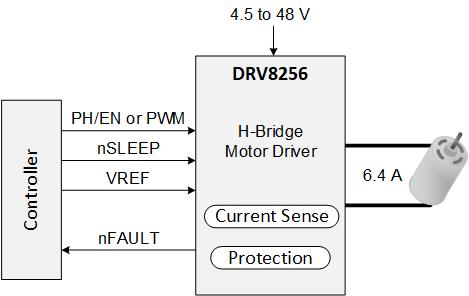
GUID-512318FB-1E10-4F50-A972-81025577F6DD-low.jpg DRV8256 Simplified Schematic