SLVSHB2
February 2024
DRV8262-Q1
PRODUCTION DATA
1
1
Features
2
Applications
3
Description
4
Pin Configuration and Functions
5
Specifications
5.1
Absolute Maximum Ratings
5.2
ESD Ratings
5.3
Recommended Operating Conditions
5.4
Thermal Information
5.4.1
Transient Thermal Impedance & Current Capability
5.5
Electrical Characteristics
5.6
Typical Characteristics
6
Detailed Description
6.1
Overview
6.2
Functional Block Diagram
6.3
Feature Description
6.4
Device Operational Modes
6.4.1
Dual H-Bridge Mode (MODE1 = 0)
6.4.2
Single H-Bridge Mode (MODE1 = 1)
6.5
Current Sensing and Regulation
6.5.1
Current Sensing and Feedback
6.5.2
Current Regulation
6.5.2.1
Mixed Decay
6.5.2.2
Smart tune Dynamic Decay
6.5.3
Current Sensing with External Resistor
6.6
Charge Pump
6.7
Linear Voltage Regulator
6.8
VCC Voltage Supply
6.9
Logic Level, Tri-Level and Quad-Level Pin Diagrams
6.10
Protection Circuits
6.10.1
VM Undervoltage Lockout (UVLO)
6.10.2
VCP Undervoltage Lockout (CPUV)
6.10.3
Logic Supply Power on Reset (POR)
6.10.4
Overcurrent Protection (OCP)
6.10.5
Thermal Shutdown (OTSD)
6.10.6
nFAULT Output
6.10.7
Fault Condition Summary
6.11
Device Functional Modes
6.11.1
Sleep Mode
6.11.2
Operating Mode
6.11.3
nSLEEP Reset Pulse
6.11.4
Functional Modes Summary
7
Application and Implementation
7.1
Application Information
7.1.1
Driving Brushed-DC Motors
7.1.1.1
Brushed-DC Motor Driver Typical Application
7.1.1.2
Power Loss Calculations - Dual H-bridge
7.1.1.3
Power Loss Calculations - Single H-bridge
7.1.1.4
Junction Temperature Estimation
7.1.1.5
Application Performance Plots
7.1.2
Driving Stepper Motors
7.1.2.1
Stepper Driver Typical Application
7.1.2.2
Power Loss Calculations
7.1.2.3
Junction Temperature Estimation
7.1.3
Driving Thermoelectric Coolers (TEC)
8
Package Thermal Considerations
8.1
DDW Package
8.1.1
Thermal Performance
8.1.1.1
Steady-State Thermal Performance
8.1.1.2
Transient Thermal Performance
8.2
PCB Material Recommendation
9
Power Supply Recommendations
9.1
Bulk Capacitance
9.2
Power Supplies
10
Layout
10.1
Layout Guidelines
10.2
Layout Example
11
Device and Documentation Support
11.1
Documentation Support
11.1.1
Related Documentation
11.2
Receiving Notification of Documentation Updates
11.3
Support Resources
11.4
Trademarks
11.5
Electrostatic Discharge Caution
11.6
Glossary
12
Revision History
13
Mechanical, Packaging, and Orderable Information
13.1
Tape and Reel Information
Package Options
Mechanical Data (Package|Pins)
DDW|44
MPDS309B
Thermal pad, mechanical data (Package|Pins)
DDW|44
PPTD374
Orderable Information
slvshb2_oa
slvshb2_pm
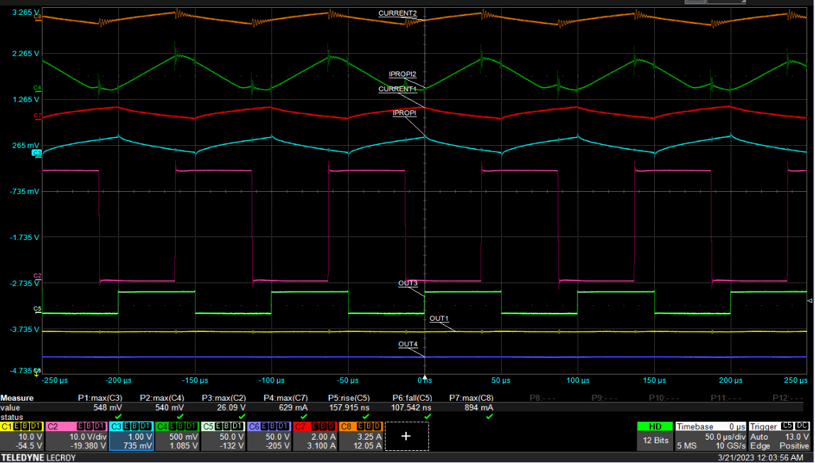
7.1.1.5
Application Performance Plots
Figure 7-3
Dual H-bridge Operation, VM = 24 V.
Traces from top to bottom: I
OUT2
, V
IPROPI2
, I
OUT1
, V
IPROPI1
, OUT2, OUT3, OUT1, OUT4