SLVSGO4 April   2022 DRV8300-Q1

PRODUCTION DATA  

  1. Features
  2. Applications
  3. Description
  4. Revision History
  5. Device Comparison Table
  6. Pin Configuration and Functions
  7. Specifications
    1. 7.1 Absolute Maximum Ratings
    2. 7.2 ESD Ratings AUTO
    3. 7.3 Recommended Operating Conditions
    4. 7.4 Thermal Information
    5. 7.5 Electrical Characteristics
    6. 7.6 Timing Diagrams
    7. 7.7 Typical Characteristics
  8. Detailed Description
    1. 8.1 Overview
    2. 8.2 Functional Block Diagram
    3. 8.3 Feature Description
      1. 8.3.1 Three BLDC Gate Drivers
        1. 8.3.1.1 Gate Drive Timings
          1. 8.3.1.1.1 Propagation Delay
          2. 8.3.1.1.2 Deadtime and Cross-Conduction Prevention
        2. 8.3.1.2 Gate Driver Outputs
      2. 8.3.2 Pin Diagrams
      3. 8.3.3 Gate Driver Protective Circuits
        1. 8.3.3.1 VBSTx Undervoltage Lockout (BSTUV)
        2. 8.3.3.2 GVDD Undervoltage Lockout (GVDDUV)
    4. 8.4 Device Functional Modes
  9. Application and Implementation
    1. 9.1 Application Information
    2. 9.2 Typical Application
      1. 9.2.1 Design Requirements
      2. 9.2.2 Bootstrap Capacitor and GVDD Capacitor Selection
      3. 9.2.3 Application Curves
  10. 10Power Supply Recommendations
  11. 11Layout
    1. 11.1 Layout Guidelines
  12. 12Device and Documentation Support
    1. 12.1 Receiving Notification of Documentation Updates
    2. 12.2 Support Resources
    3. 12.3 Trademarks
    4. 12.4 Electrostatic Discharge Caution
    5. 12.5 Glossary
  13. 13Mechanical, Packaging, and Orderable Information

Package Options

Mechanical Data (Package|Pins)
Thermal pad, mechanical data (Package|Pins)
Orderable Information
Deadtime and Cross-Conduction Prevention

In the DRV8300-Q1, high-side and low-side inputs operate independently, with an exception to prevent cross conduction when high and low side are turned ON at same time. The DRV8300-Q1 turns OFF high-side and low-side output to prevent shoot through when the both high-side and low-side inputs are at logic HIGH at same time.

Fixed deadtime of 215 ns (typical value) is inserted to prevent high and low side gate output turning ON at same time.
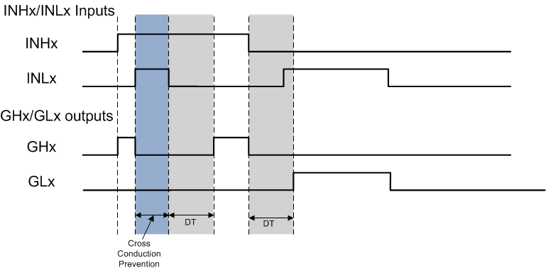
GUID-F1F8F7D0-544C-4DFE-AF93-03A2015BBBA7-low.gif Figure 8-2 Cross Conduction Prevention and Deadtime Insertion