SLVSFG5D September 2020 – March 2022 DRV8300
PRODUCTION DATA
- 1 Features
- 2 Applications
- 3 Description
- 4 Revision History
- 5 Device Comparison Table
- 6 Pin Configuration and Functions
- 7 Specifications
- 8 Detailed Description
- 9 Application and Implementation
- 10Power Supply Recommendations
- 11Layout
- 12Device and Documentation Support
- 13Mechanical, Packaging, and Orderable Information
Package Options
Mechanical Data (Package|Pins)
Thermal pad, mechanical data (Package|Pins)
- RGE|24
Orderable Information
3 Description
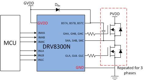
DRV8300 is 100-V three half-bridge gate drivers, capable of driving high-side and low-side N-channel power MOSFETs. The DRV8300D generates the correct gate drive voltages using an integrated bootstrap diode and external capacitor for the high-side MOSFETs. The DRV8300N generates the correct gate drive voltages using an external bootstrap diode and external capacitor for the high-side MOSFETs. GVDD is used to generate gate drive voltage for the low-side MOSFETs. The Gate Drive architecture supports peak up to 750-mA source and 1.5-A sink currents.
The phase pins SHx is able to tolerate the significant negative voltage transients; while high side gate driver supply BSTx and GHx is able to support to higher positive voltage transients (125-V) abs max voltage which improves robustness of the system. Small propagation delay and delay matching specifications minimize the dead-time requirement which further improves efficiency. Undervoltage protection is provided for both low and high side through GVDD and BST undervoltage lockout.
| PART NUMBER | PACKAGE | BODY SIZE (NOM) |
|---|---|---|
| DRV8300DIPW | TSSOP (20) | 6.40 mm × 4.40 mm |
| DRV8300DPW | TSSOP (20) | 6.40 mm × 4.40 mm |
| DRV8300NIPW | TSSOP (20) | 6.40 mm × 4.40 mm |
| DRV8300NPW | TSSOP (20) | 6.40 mm × 4.40 mm |
| DRV8300DRGE | VQFN (24) | 4.00 mm × 4.00 mm |
| DRV8300NRGE | VQFN (24) | 4.00 mm × 4.00 mm |
 Simplified Schematic for DRV8300D
 Simplified Schematic for DRV8300N