SLOS842A September 2013 – June 2015 DRV8301-Q1
PRODUCTION DATA.
- 1 Features
- 2 Applications
- 3 Description
- 4 Revision History
- 5 Pin Configuration and Functions
-
6 Specifications
- 6.1 Absolute Maximum Ratings
- 6.2 ESD Ratings
- 6.3 Recommended Operating Conditions
- 6.4 Thermal Information
- 6.5 Electrical Characteristics
- 6.6 Buck Converter Characteristics
- 6.7 Current Shunt Amplifier Characteristics
- 6.8 Gate Timing and Protection Characteristics
- 6.9 SPI Timing Requirements (Slave Mode Only)
- 6.10 Typical Characteristics
- 7 Detailed Description
- 8 Application and Implementation
- 9 Power Supply Recommendations
- 10Layout
- 11Device and Documentation Support
- 12Mechanical, Packaging, and Orderable Information
Package Options
Mechanical Data (Package|Pins)
- DCA|56
Thermal pad, mechanical data (Package|Pins)
- DCA|56
Orderable Information
6 Specifications
6.1 Absolute Maximum Ratings
over operating free-air temperature range (unless otherwise noted)(1)(1) Stresses beyond those listed under Absolute Maximum Ratings may cause permanent damage to the device. These are stress ratings only, which do not imply functional operation of the device at these or any other conditions beyond those indicated under Recommended Operating Conditions. Exposure to absolute-maximum-rated conditions for extended periods may affect device reliability.
6.2 ESD Ratings
| VALUE | UNIT | |||||
|---|---|---|---|---|---|---|
| V(ESD) | Electrostatic discharge | Human body model (HBM), per AEC Q100-002(1) | ±2000 | V | ||
| Charged device model (CDM), per AEC Q100-011 | Corner pins (1, 28, 56, and 29) | ±500 | ||||
| Other pins | ±500 | |||||
(1) AEC Q100-002 indicates HBM stressing is done in accordance with the ANSI/ESDA/JEDEC JS-001 specification.
6.3 Recommended Operating Conditions
| MIN | NOM | MAX | UNIT | |||
|---|---|---|---|---|---|---|
| VPVDD1 | DC supply voltage PVDD1 for normal operation | Relative to PGND | 6 | 60 | V | |
| VPVDD2 | DC supply voltage PVDD2 for buck converter | 3.5 | 60 | V | ||
| IDIN_EN | Input current of digital pins when EN_GATE is high | 100 | µA | |||
| IDIN_DIS | Input current of digital pins when EN_GATE is low | 1 | µA | |||
| CDIN | Maximum capacitance on digital input pin | 10 | pF | |||
| CO_OPA | Maximum output capacitance on outputs of shunt amplifier | 20 | pF | |||
| RDTC | Dead time control resistor range. Time range is 50 ns (-GND) to 500 ns (150 kΩ) with a linear approximation. | 0 | 150 | kΩ | ||
| IFAULT | FAULT pin sink current. Open drain | V = 0.4 V | 2 | mA | ||
| IOCTW | OCTW pin sink current. Open drain | V = 0.4 V | 2 | mA | ||
| VREF | External voltage reference voltage for current shunt amplifiers | 2 | 6 | V | ||
| fgate | Operating switching frequency of gate driver | Qg(TOT) = 25 nC or total 30-mA gate drive average current | 200 | kHz | ||
| Igate | Total average gate drive current | 30 | mA | |||
| TA | Ambient temperature | –40 | 125 | °C | ||
6.4 Thermal Information
| THERMAL METRIC(1) | DRV8301-Q1 | UNIT | |
|---|---|---|---|
| DCA (HTSSOP) | |||
| 56 PINS | |||
| RθJA | Junction-to-ambient thermal resistance | 30.3 | °C/W |
| RθJC(top) | Junction-to-case (top) thermal resistance | 33.5 | °C/W |
| RθJB | Junction-to-board thermal resistance | 17.5 | °C/W |
| ψJT | Junction-to-top characterization parameter | 0.9 | °C/W |
| ψJB | Junction-to-board characterization parameter | 7.2 | °C/W |
| RθJC(bot) | Junction-to-case (bottom) thermal resistance | 0.9 | °C/W |
(1) For more information about traditional and new thermal metrics, see the Semiconductor and IC Package Thermal Metrics application report, SPRA953.
6.5 Electrical Characteristics
PVDD = 6 to 60 V, TC = 25°C, unless specified under test condition| PARAMETER | TEST CONDITIONS | MIN | TYP | MAX | UNIT | |
|---|---|---|---|---|---|---|
| INPUT PINS: INH_X, INL_X, nSCS, SDI, SCLK, EN_GATE, DC_CAL | ||||||
| VIH | High input threshold | 2 | V | |||
| VIL | Low input threshold | 0.8 | V | |||
| RPULL_DOWN – INTERNAL PULLDOWN RESISTOR FOR GATE DRIVER INPUTS | ||||||
| REN_GATE | Internal pulldown resistor for EN_GATE | 100 | kΩ | |||
| RINH_X | Internal pulldown resistor for high-side PWMs (INH_A, INH_B, and INH_C) | EN_GATE high | 100 | kΩ | ||
| RINH_X | Internal pulldown resistor for low-side PWMs (INL_A, INL_B, and INL_C) | EN_GATE high | 100 | kΩ | ||
| RnSCS | Internal pulldown resistor for SCS | EN_GATE high | 100 | kΩ | ||
| RSDI | Internal pulldown resistor for SDI | EN_GATE high | 100 | kΩ | ||
| RDC_CAL | Internal pulldown resistor for DC_CAL | EN_GATE high | 100 | kΩ | ||
| RSCLK | Internal pulldown resistor for SCLK | EN_GATE high | 100 | kΩ | ||
| OUTPUT PINS: nFAULT AND nOCTW | ||||||
| VOL | Low output threshold | IO = 2 mA | 0.4 | V | ||
| VOH | High-output threshold | External 47 kΩ pullup resistor connected to 3-5.5 V | 2.4 | V | ||
| IOH | Leakage Current on Open-Drain Pins When Logic High FAULT and OCTW) | 1 | µA | |||
| GATE DRIVE OUTPUT: GH_A, GH_B, GH_C, GL_A, GL_B, GL_C | ||||||
| VGX_NORM | Gate driver Vgs voltage | PVDD = 8 to 60 V, Igate = 30 mA, CCP = 22 nF |
9.5 | 11.5 | V | |
| PVDD = 8 to 60 V, Igate = 30 mA, CCP = 220 nF |
9.5 | 11.5 | ||||
| VGX_MIN | Gate driver Vgs voltage | PVDD = 6 to 8 V, Igate = 15 mA, CCP = 22 nF |
8.8 | V | ||
| PVDD = 6 to 8 V, Igate = 30 mA, CCP = 220 nF |
8.3 | |||||
| Ioso1 | Maximum source current setting 1, peak | Vgs of FET equals to 2 V. REG 0x02 | 1.7 | A | ||
| Iosi1 | Maximum sink current setting 1, peak | Vgs of FET equals to 8 V. REG 0x02 | 2.3 | A | ||
| Ioso2 | Source current setting 2, peak | Vgs of FET equals to 2 V. REG 0x02 | 0.7 | A | ||
| Iosi2 | Sink current setting 2, peak | Vgs of FET equals to 8 V. REG 0x02 | 1 | A | ||
| Ioso3 | Source current setting 3, peak | Vgs of FET equals to 2 V. REG 0x02 | 0.25 | A | ||
| Iosi3 | Sink current setting 3, peak | Vgs of FET equals to 8 V. REG 0x02 | 0.5 | A | ||
| Rgate_off | Gate output impedence during standby mode when EN_GATE low (pins GH_x, GL_x) | 1.6 | 2.4 | kΩ | ||
| SUPPLY CURRENTS | ||||||
| IPVDD1_STB | PVDD1 supply current, standby | EN_GATE is low. PVDD1 = 8 V. | 20 | 50 | µA | |
| IPVDD1_OP | PVDD1 supply current, operating | EN_GATE is high, no load on gate drive output, switching at 10 kHz, 100-nC gate charge |
15 | mA | ||
| IPVDD1_HIZ | PVDD1 Supply current, Hi-Z | EN_GATE is high, gate not switching | 2 | 5 | 10 | mA |
| INTERNAL REGULATOR VOLTAGE | ||||||
| AVDD | AVDD voltage | PVDD = 8 to 60 V | 6 | 6.5 | 7 | V |
| PVDD = 6 to 60 V | 5.5 | 6 | ||||
| DVDD | DVDD voltage | 3 | 3.3 | 3.6 | V | |
| VOLTAGE PROTECTION | ||||||
| VPVDD_UV | Undervoltage protection limit, PVDD | PVDD falling | 5.9 | V | ||
| PVDD rising | 6 | |||||
| VGVDD_UV | Undervoltage protection limit, GVDD | GVDD falling | 7.5 | V | ||
| VGVDD_OV | Overvoltage protection limit, GVDD | 16 | V | |||
| CURRENT PROTECTION, (VDS SENSING) | ||||||
| VDS_OC | Drain-source voltage protection limit | PVDD = 8 to 60 V | 0.125 | 2.4 | V | |
| PVDD = 6 to 8 V(1) | 0.125 | 1.491 | ||||
| Toc | OC sensing response time | 1.5 | µs | |||
| TOC_PULSE | OCTW pin reporting pulse stretch length for OC event | 64 | µs | |||
(1) Reduced AVDD voltage range results in limitations on settings for overcurrent protection. See Table 11.
6.6 Buck Converter Characteristics
TC = 25°C unless otherwise specified| PARAMETER | TEST CONDITIONS | MIN | TYP | MAX | UNIT | |
|---|---|---|---|---|---|---|
| VUVLO | Internal undervoltage lockout threshold | No voltage hysteresis, rising and falling | 2.5 | V | ||
| ISD(PVDD2) | Shutdown supply current | EN = 0 V, 25°C, 3.5 V ≤ VIN ≤ 60 V | 1.3 | 4 | µA | |
| INON_SW(PVDD2) | Operating: nonswitching supply current | VSENSE = 0.83 V, VIN = 12 V | 116 | 136 | µA | |
| VEN_BUCK | Enable threshold voltage | No voltage hysteresis, rising and falling, 25°C | 0.9 | 1.25 | 1.55 | V |
| RDS_ON | On-resistance | VIN = 3.5 V, BOOT-PH = 3 V | 300 | mΩ | ||
| ILIM | Current limit threshold | VIN = 12 V, TJ = 25°C | 1.8 | 2.7 | A | |
| Fsw | Switching frequency | RT = 200 kΩ | 450 | 581 | 720 | kHz |
| PWRGD | VSENSE threshold | VSENSE falling | 92% | |||
| VSENSE rising | 94% | |||||
| VSENSE rising | 109% | |||||
| VSENSE falling | 107% | |||||
| Hysteresis | VSENSE falling | 2% | ||||
| Output high leakage | VSENSE = VREF, V(PWRGD) = 5.5 V, 25°C | 10 | nA | |||
| On resistance | I(PWRGD) = 3 mA, VSENSE < 0.79 V | 50 | Ω | |||
6.7 Current Shunt Amplifier Characteristics
TC = 25°C unless otherwise specified| PARAMETER | TEST CONDITIONS | MIN | TYP | MAX | UNIT | |
|---|---|---|---|---|---|---|
| G1 | Gain option 1 | Tc = –40°C to 125°C | 9.5 | 10 | 10.5 | V/V |
| G2 | Gain option 2 | Tc = –40°C to 125°C | 18 | 20 | 21 | V/V |
| G3 | Gain Option 3 | Tc = –40°C to 125°C | 38 | 40 | 42 | V/V |
| G4 | Gain Option 4 | Tc = –40°C to 125°C | 75 | 80 | 85 | V/V |
| Tsettling | Settling time to 1% | Tc = 0-60°C, G = 10, Vstep = 2 V | 300 | ns | ||
| Tsettling | Settling time to 1% | Tc = 0-60°C, G = 20, Vstep = 2 V | 600 | ns | ||
| Tsettling | Settling time to 1% | Tc = 0-60°C, G = 40, Vstep = 2 V | 1.2 | µs | ||
| Tsettling | Settling time to 1% | Tc = 0-60°C, G = 80, Vstep = 2 V | 2.4 | µs | ||
| Vswing | Output swing linear range | 0.3 | 5.7 | V | ||
| Slew Rate | G = 10 | 10 | V/µs | |||
| DC_offset | Offset error RTI | G = 10 with input shorted | 4 | mV | ||
| Drift_offset | Offset drift RTI | 10 | µV/C | |||
| Ibias | Input bias current | 100 | µA | |||
| Vin_com | Common input mode range | –0.15 | 0.15 | V | ||
| Vin_dif | Differential input range | –0.3 | 0.3 | V | ||
| Vo_bias | Output bias | With zero input current, VREF up to 6 V | –0.5% | 0.5 × VREF | 0.5% | V |
| CMRR_OV | Overall CMRR with gain resistor mismatch | CMRR at DC, gain = 10 | 70 | 85 | dB | |
6.8 Gate Timing and Protection Characteristics
| PARAMETER | TEST CONDITIONS | MIN | TYP | MAX | UNIT | |
|---|---|---|---|---|---|---|
| TIMING, OUTPUT PINS | ||||||
| tpd,If-O | Positive input falling to GH_x falling | CL = 1 nF, 50% to 50% | 45 | ns | ||
| tpd,Ir-O | Positive input rising to GL_x falling | CL = 1 nF, 50% to 50% | 45 | ns | ||
| Td_min | Minimum dead time after hand shaking(1) | 50 | ns | |||
| Tdtp | Dead Time | With RDTC set to different values | 50 | 500 | ns | |
| tGDr | Rise time, gate drive output | CL = 1 nF, 10% to 90% | 25 | ns | ||
| tGDF | Fall time, gate drive output | CL = 1 nF, 90% to 10% | 25 | ns | ||
| TON_MIN | Minimum on pulse | Not including handshake communication. Hi-z to on state, output of gate driver | 50 | ns | ||
| Tpd_match | Propagation delay matching between high-side and low-side | 5 | ns | |||
| Tdt_match | Deadtime matching | 5 | ns | |||
| TIMING, PROTECTION AND CONTROL | ||||||
| tpd,R_GATE-OP | Start-up time, from EN_GATE active high to device ready for normal operation | PVDD is up before start-up, all charge pump caps and regulator caps as in recommended condition | 5 | 10 | ms | |
| tpd,R_GATE-Quick | If EN_GATE goes from high to low and back to high state within quick reset time, it will only reset all faults and gate driver without powering down charge pump, current amp, and related internal voltage regulators. | Maximum low pulse time | 10 | µs | ||
| tpd,E-L | Delay, error event to all gates low | 200 | ns | |||
| tpd,E-FAULT | Delay, error event to FAULT low | 200 | ns | |||
| OTW_CLR | Junction temperature for resetting over temperature warning | 115 | °C | |||
| OTW_SET/OTSD_CLR | Junction temperature for over temperature warning and resetting over temperature shut down | 130 | °C | |||
| OTSD_SET | Junction temperature for over temperature shut down | 150 | °C | |||
(1) Dead time programming definition: Adjustable delay from GH_x falling edge to GL_X rising edge, and GL_X falling edge to GH_X rising edge. This is a minimum dead-time insertion. It is not added to the value set by the microcontroller externally.
6.9 SPI Timing Requirements (Slave Mode Only)
See Figure 1 and Figure 2.| MIN | NOM | MAX | UNIT | |||
|---|---|---|---|---|---|---|
| tSPI_READY | SPI ready after EN_GATE transitions to HIGH | PVDD > 6 V | 5 | 10 | ms | |
| tCLK | Minimum SPI clock period | 100 | ns | |||
| tCLKH | Clock high time | 40 | ns | |||
| tCLKL | Clock low time | 40 | ns | |||
| tSU_SDI | SDI input data setup time | 20 | ns | |||
| tHD_SDI | SDI input data hold time | 30 | ns | |||
| tD_SDO | SDO output data delay time, CLK high to SDO valid | CL = 20 pF | 20 | ns | ||
| tHD_SDO | SDO output data hold time | 40 | ns | |||
| tSU_SCS | SCS setup time | 50 | ns | |||
| tHD_SCS | SCS hold time | 50 | ns | |||
| tHI_SCS | SCS minimum high time before SCS active low | 40 | ns | |||
| tACC | SCS access time, SCS low to SDO out of high impedance | 10 | ns | |||
| tDIS | SCS disable time, SCS high to SDO high impedance | 10 | ns | |||
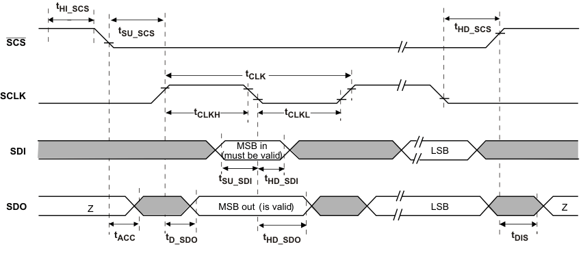 Figure 1. SPI Slave Mode Timing Definition
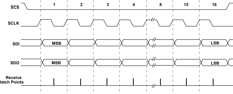 Figure 2. SPI Slave Mode Timing Diagram
6.10 Typical Characteristics
