SLVSE39B November 2017 – July 2018 DRV8304
UNLESS OTHERWISE NOTED, this document contains PRODUCTION DATA.
- 1 Features
- 2 Applications
- 3 Description
- 4 Revision History
- 5 Pin Configuration and Functions
- 6 Specifications
-
7 Detailed Description
- 7.1 Overview
- 7.2 Functional Block Diagram
- 7.3
Feature Description
- 7.3.1 3-Phase Smart Gate Drivers
- 7.3.2 DVDD Linear Voltage Regulator
- 7.3.3 Pin Diagrams
- 7.3.4 Low-Side Current-Shunt Amplifiers
- 7.3.5 Gate-Driver Protection Circuits
- 7.4 Device Functional Modes
- 7.5 Programming
- 7.6
Register Maps
- Table 1. DRV8304S Register Map
- 7.6.1 Status Registers (DRV8304S Only)
- 7.6.2
Control Registers (DRV8304S Only)
- 7.6.2.1 Driver Control Register (Address = 0x02) [reset = 0x00]
- 7.6.2.2 Gate Drive HS Register (Address = 0x03) [reset = 0x377]
- 7.6.2.3 Gate Drive LS Register (Address = 0x04) [reset = 0x777]
- 7.6.2.4 OCP Control Register (Address = 0x05) [reset = 0x145]
- 7.6.2.5 CSA Control Register (Address = 0x06) [reset = 0x283]
- 8 Application and Implementation
- 9 Power Supply Recommendations
- 10Layout
- 11Device and Documentation Support
- 12Mechanical, Packaging, and Orderable Information
Package Options
Refer to the PDF data sheet for device specific package drawings
Mechanical Data (Package|Pins)
- RHA|40
Thermal pad, mechanical data (Package|Pins)
- RHA|40
Orderable Information
7.3.3 Pin Diagrams
Figure 25 shows the input structure for the logic-level pins, INHx, INLx, CAL, nSCS, SCLK, and SDI. The input can be driven with a voltage or external resistor.
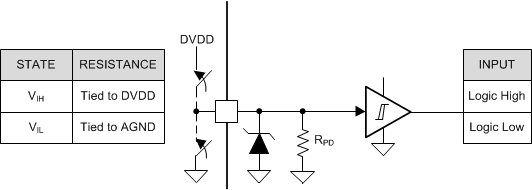 Figure 25. Logic-Level Input Pin Structure (INHx, INLx, CAL, nSCS, SCLK, and SDI)
 Figure 26 shows the input structure for the logic-level ENABLE pin. The input can be driven with a voltage or external resistor. The ENABLE pin is latched when the device is powered-up.
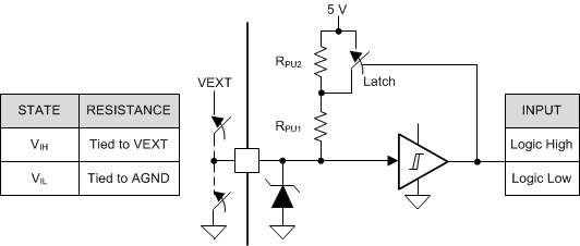 Figure 26. Logic-Level Input Pin Structure (ENABLE)
 Figure 27 shows the structure of the four-level input pins, MODE and GAIN, on the hardware interface device. The input can be set with an external resistor. The MODE and GAIN pins are latched when the device is powered-up.
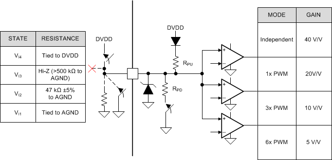 Figure 27. Four-Level Input Pin Structure (MODE and GAIN)
 Figure 28 shows the structure of the seven-level input pins, IDRIVE and VDS, on the hardware interface device. The input can be set with an external resistor. The IDRIVE and VDS pins are latched when the device is powered-up.
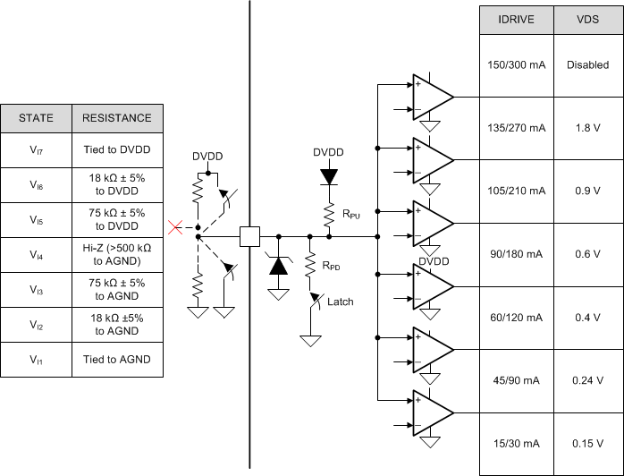 Figure 28. Seven-Level Input Pin Structure (IDRIVE and VDS)
 Figure 29 shows the structure of the open-drain output pin, nFAULT. The open-drain output requires an external pullup resistor to function properly.
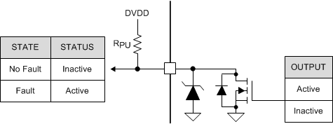 Figure 29. Open-Drain Output Pin Structure