SLVSE38A April   2018  – July 2018 DRV8306

PRODUCTION DATA.  

  1. Features
  2. Applications
  3. Description
    1.     Simplified Schematic
  4. Revision History
  5. Pin Configuration and Functions
    1.     Pin Functions
  6. Specifications
    1. 6.1 Absolute Maximum Ratings
    2. 6.2 ESD Ratings
    3. 6.3 Recommended Operating Conditions
    4. 6.4 Thermal Information
    5. 6.5 Electrical Characteristics
    6. 6.6 Typical Characteristics
  7. Detailed Description
    1. 7.1 Overview
    2. 7.2 Functional Block Diagram
    3. 7.3 Feature Description
      1. 7.3.1 Three Phase Smart Gate Drivers
        1. 7.3.1.1 PWM Control Mode (1x PWM Mode)
        2. 7.3.1.2 Hardware Interface Mode
        3. 7.3.1.3 Gate Driver Voltage Supplies
        4. 7.3.1.4 Smart Gate Drive Architecture
          1. 7.3.1.4.1 IDRIVE: MOSFET Slew-Rate Control
          2. 7.3.1.4.2 TDRIVE: MOSFET Gate Drive Control
          3. 7.3.1.4.3 Gate Drive Clamp
          4. 7.3.1.4.4 Propagation Delay
          5. 7.3.1.4.5 MOSFET VDS Monitors
          6. 7.3.1.4.6 VDRAIN Sense Pin
      2. 7.3.2 DVDD Linear Voltage Regulator
      3. 7.3.3 Pulse-by-Pulse Current Limit
      4. 7.3.4 Hall Comparators
      5. 7.3.5 FGOUT Signal
      6. 7.3.6 Pin Diagrams
      7. 7.3.7 Gate-Driver Protective Circuits
        1. 7.3.7.1 VM Supply Undervoltage Lockout (UVLO)
        2. 7.3.7.2 VCP Charge-Pump Undervoltage Lockout (CPUV)
        3. 7.3.7.3 MOSFET VDS Overcurrent Protection (VDS_OCP)
        4. 7.3.7.4 VSENSE Overcurrent Protection (SEN_OCP)
        5. 7.3.7.5 Gate Driver Fault (GDF)
        6. 7.3.7.6 Thermal Shutdown (OTSD)
    4. 7.4 Device Functional Modes
      1. 7.4.1 Gate Driver Functional Modes
        1. 7.4.1.1 Sleep Mode
        2. 7.4.1.2 Operating Mode
        3. 7.4.1.3 Fault Reset (ENABLE Reset Pulse)
  8. Application and Implementation
    1. 8.1 Application Information
      1. 8.1.1 Hall Sensor Configuration and Connection
        1. 8.1.1.1 Typical Configuration
        2. 8.1.1.2 Open Drain Configuration
        3. 8.1.1.3 Series Configuration
        4. 8.1.1.4 Parallel Configuration
    2. 8.2 Typical Application
      1. 8.2.1 Primary Application
        1. 8.2.1.1 Design Requirements
        2. 8.2.1.2 Detailed Design Procedure
          1. 8.2.1.2.1 External MOSFET Support
            1. 8.2.1.2.1.1 Example
          2. 8.2.1.2.2 IDRIVE Configuration
            1. 8.2.1.2.2.1 Example
          3. 8.2.1.2.3 VDS Overcurrent Monitor Configuration
            1. 8.2.1.2.3.1 Example
        3. 8.2.1.3 Application Curves
  9. Power Supply Recommendations
    1. 9.1 Bulk Capacitance Sizing
  10. 10Layout
    1. 10.1 Layout Guidelines
    2. 10.2 Layout Example
  11. 11Device and Documentation Support
    1. 11.1 Device Support
      1. 11.1.1 Device Nomenclature
    2. 11.2 Documentation Support
      1. 11.2.1 Related Documentation
    3. 11.3 Receiving Notification of Documentation Updates
    4. 11.4 Community Resources
    5. 11.5 Trademarks
    6. 11.6 Electrostatic Discharge Caution
    7. 11.7 Glossary
  12. 12Mechanical, Packaging, and Orderable Information

Package Options

Mechanical Data (Package|Pins)
Thermal pad, mechanical data (Package|Pins)
Orderable Information

Hall Comparators

Three comparators are provided to process the raw signals from the Hall effect transducers to commutate the motor. The Hall comparators sense zero crossings of the differential inputs and pass the information to digital logic. The Hall comparators have hysteresis, and their detect threshold is centered at 0. The hysteresis is defined as shown in Figure 20.

In addition to the hysteresis, the Hall inputs are deglitched with a circuit that ignores any extra Hall transitions for a period of tHDEG after sensing a valid transition. Ignoring these transitions for the tHDEG time prevents PWM noise from being coupled into the Hall inputs, which can result in erroneous commutation.

If excessive noise is still coupled into the Hall comparator inputs, adding capacitors between the positive and negative inputs of the Hall comparators may be required. The ESD protection circuitry on the Hall inputs implements a diode to the DVDD pin. Because of this diode, the voltage on the Hall inputs should not exceed the DVDD voltage.

Because the DVDD pin is disabled in standby mode (ENABLE inactive), the Hall inputs should not be driven by external voltages in standby mode. If the Hall sensors are powered externally, the supply to the Hall sensors should be disabled if the DRV8306 device is put into standby mode. In addition, the Hall sensor power supply should be powered up after enabling the motor otherwise an invalid Hall state may cause a delay in motor operation.
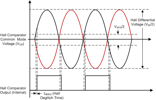
DRV8306 drv8306-hall-comparators.gifFigure 20. Hall Comparators