SLVSE38A
April 2018 – July 2018
DRV8306
PRODUCTION DATA.
1
Features
2
Applications
3
Description
Simplified Schematic
4
Revision History
5
Pin Configuration and Functions
Pin Functions
6
Specifications
6.1
Absolute Maximum Ratings
6.2
ESD Ratings
6.3
Recommended Operating Conditions
6.4
Thermal Information
6.5
Electrical Characteristics
6.6
Typical Characteristics
7
Detailed Description
7.1
Overview
7.2
Functional Block Diagram
7.3
Feature Description
7.3.1
Three Phase Smart Gate Drivers
7.3.1.1
PWM Control Mode (1x PWM Mode)
7.3.1.2
Hardware Interface Mode
7.3.1.3
Gate Driver Voltage Supplies
7.3.1.4
Smart Gate Drive Architecture
7.3.1.4.1
IDRIVE: MOSFET Slew-Rate Control
7.3.1.4.2
TDRIVE: MOSFET Gate Drive Control
7.3.1.4.3
Gate Drive Clamp
7.3.1.4.4
Propagation Delay
7.3.1.4.5
MOSFET VDS Monitors
7.3.1.4.6
VDRAIN Sense Pin
7.3.2
DVDD Linear Voltage Regulator
7.3.3
Pulse-by-Pulse Current Limit
7.3.4
Hall Comparators
7.3.5
FGOUT Signal
7.3.6
Pin Diagrams
7.3.7
Gate-Driver Protective Circuits
7.3.7.1
VM Supply Undervoltage Lockout (UVLO)
7.3.7.2
VCP Charge-Pump Undervoltage Lockout (CPUV)
7.3.7.3
MOSFET VDS Overcurrent Protection (VDS_OCP)
7.3.7.4
VSENSE Overcurrent Protection (SEN_OCP)
7.3.7.5
Gate Driver Fault (GDF)
7.3.7.6
Thermal Shutdown (OTSD)
7.4
Device Functional Modes
7.4.1
Gate Driver Functional Modes
7.4.1.1
Sleep Mode
7.4.1.2
Operating Mode
7.4.1.3
Fault Reset (ENABLE Reset Pulse)
8
Application and Implementation
8.1
Application Information
8.1.1
Hall Sensor Configuration and Connection
8.1.1.1
Typical Configuration
8.1.1.2
Open Drain Configuration
8.1.1.3
Series Configuration
8.1.1.4
Parallel Configuration
8.2
Typical Application
8.2.1
Primary Application
8.2.1.1
Design Requirements
8.2.1.2
Detailed Design Procedure
8.2.1.2.1
External MOSFET Support
8.2.1.2.1.1
Example
8.2.1.2.2
IDRIVE Configuration
8.2.1.2.2.1
Example
8.2.1.2.3
VDS Overcurrent Monitor Configuration
8.2.1.2.3.1
Example
8.2.1.3
Application Curves
9
Power Supply Recommendations
9.1
Bulk Capacitance Sizing
10
Layout
10.1
Layout Guidelines
10.2
Layout Example
11
Device and Documentation Support
11.1
Device Support
11.1.1
Device Nomenclature
11.2
Documentation Support
11.2.1
Related Documentation
11.3
Receiving Notification of Documentation Updates
11.4
Community Resources
11.5
Trademarks
11.6
Electrostatic Discharge Caution
11.7
Glossary
12
Mechanical, Packaging, and Orderable Information
Package Options
Mechanical Data (Package|Pins)
RSM|32
MPQF195B
Thermal pad, mechanical data (Package|Pins)
RSM|32
QFND112H
Orderable Information
slvse38a_oa
slvse38a_pm
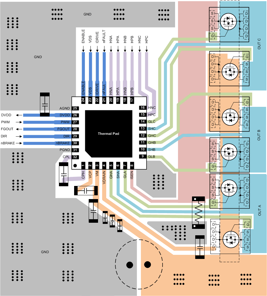
10.2
Layout Example
Figure 44.
Layout Example