SLVSE38A April   2018  – July 2018 DRV8306

PRODUCTION DATA.  

  1. Features
  2. Applications
  3. Description
    1.     Simplified Schematic
  4. Revision History
  5. Pin Configuration and Functions
    1.     Pin Functions
  6. Specifications
    1. 6.1 Absolute Maximum Ratings
    2. 6.2 ESD Ratings
    3. 6.3 Recommended Operating Conditions
    4. 6.4 Thermal Information
    5. 6.5 Electrical Characteristics
    6. 6.6 Typical Characteristics
  7. Detailed Description
    1. 7.1 Overview
    2. 7.2 Functional Block Diagram
    3. 7.3 Feature Description
      1. 7.3.1 Three Phase Smart Gate Drivers
        1. 7.3.1.1 PWM Control Mode (1x PWM Mode)
        2. 7.3.1.2 Hardware Interface Mode
        3. 7.3.1.3 Gate Driver Voltage Supplies
        4. 7.3.1.4 Smart Gate Drive Architecture
          1. 7.3.1.4.1 IDRIVE: MOSFET Slew-Rate Control
          2. 7.3.1.4.2 TDRIVE: MOSFET Gate Drive Control
          3. 7.3.1.4.3 Gate Drive Clamp
          4. 7.3.1.4.4 Propagation Delay
          5. 7.3.1.4.5 MOSFET VDS Monitors
          6. 7.3.1.4.6 VDRAIN Sense Pin
      2. 7.3.2 DVDD Linear Voltage Regulator
      3. 7.3.3 Pulse-by-Pulse Current Limit
      4. 7.3.4 Hall Comparators
      5. 7.3.5 FGOUT Signal
      6. 7.3.6 Pin Diagrams
      7. 7.3.7 Gate-Driver Protective Circuits
        1. 7.3.7.1 VM Supply Undervoltage Lockout (UVLO)
        2. 7.3.7.2 VCP Charge-Pump Undervoltage Lockout (CPUV)
        3. 7.3.7.3 MOSFET VDS Overcurrent Protection (VDS_OCP)
        4. 7.3.7.4 VSENSE Overcurrent Protection (SEN_OCP)
        5. 7.3.7.5 Gate Driver Fault (GDF)
        6. 7.3.7.6 Thermal Shutdown (OTSD)
    4. 7.4 Device Functional Modes
      1. 7.4.1 Gate Driver Functional Modes
        1. 7.4.1.1 Sleep Mode
        2. 7.4.1.2 Operating Mode
        3. 7.4.1.3 Fault Reset (ENABLE Reset Pulse)
  8. Application and Implementation
    1. 8.1 Application Information
      1. 8.1.1 Hall Sensor Configuration and Connection
        1. 8.1.1.1 Typical Configuration
        2. 8.1.1.2 Open Drain Configuration
        3. 8.1.1.3 Series Configuration
        4. 8.1.1.4 Parallel Configuration
    2. 8.2 Typical Application
      1. 8.2.1 Primary Application
        1. 8.2.1.1 Design Requirements
        2. 8.2.1.2 Detailed Design Procedure
          1. 8.2.1.2.1 External MOSFET Support
            1. 8.2.1.2.1.1 Example
          2. 8.2.1.2.2 IDRIVE Configuration
            1. 8.2.1.2.2.1 Example
          3. 8.2.1.2.3 VDS Overcurrent Monitor Configuration
            1. 8.2.1.2.3.1 Example
        3. 8.2.1.3 Application Curves
  9. Power Supply Recommendations
    1. 9.1 Bulk Capacitance Sizing
  10. 10Layout
    1. 10.1 Layout Guidelines
    2. 10.2 Layout Example
  11. 11Device and Documentation Support
    1. 11.1 Device Support
      1. 11.1.1 Device Nomenclature
    2. 11.2 Documentation Support
      1. 11.2.1 Related Documentation
    3. 11.3 Receiving Notification of Documentation Updates
    4. 11.4 Community Resources
    5. 11.5 Trademarks
    6. 11.6 Electrostatic Discharge Caution
    7. 11.7 Glossary
  12. 12Mechanical, Packaging, and Orderable Information

Package Options

Mechanical Data (Package|Pins)
Thermal pad, mechanical data (Package|Pins)
Orderable Information

Smart Gate Drive Architecture

The DRV8306 gate drivers use an adjustable, complimentary, push-pull topology for both the high-side and low-side drivers. This topology allows for both a strong pullup and pulldown of the external MOSFET gates.

Additionally, the gate drivers use a smart gate-drive architecture to provide additional control of the external power MOSFETs, take additional steps to protect the MOSFETs, and allow for optimal tradeoffs between efficiency and robustness. This architecture is implemented through two components called IDRIVE and TDRIVE which are detailed in the IDRIVE: MOSFET Slew-Rate Control section and TDRIVE: MOSFET Gate Drive Control section. Figure 12 shows the high-level functional block diagram of the gate driver.

The IDRIVE gate-drive current and TDRIVE gate-drive time should be initially selected based on the parameters of the external power MOSFET used in the system and the desired rise and fall times (see the Application and Implementation section).

The high-side gate driver also implements a Zener clamp diode to help protect the external MOSFET gate from overvoltage conditions in the case of external short-circuit events on the MOSFET.
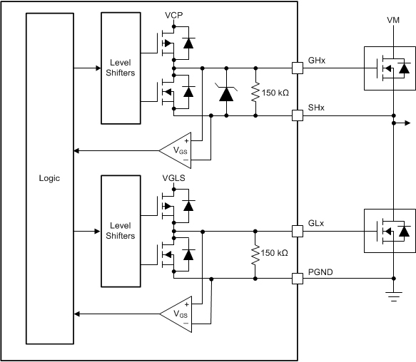
DRV8306 drv8306-gate-driver-block-diagram.gifFigure 12. Gate Driver Block Diagram