SLVSH52 February   2023 DRV8316C-Q1

PRODUCTION DATA  

  1. Features
  2. Applications
  3. Description
  4. Revision History
  5. Device Comparison Table
  6. Pin Configuration and Functions
  7. Specifications
    1. 7.1 Absolute Maximum Ratings
    2. 7.2 ESD Ratings Auto
    3. 7.3 Recommended Operating Conditions
    4. 7.4 Thermal Information
    5. 7.5 Electrical Characteristics
    6. 7.6 SPI Timing Requirements
    7. 7.7 SPI Slave Mode Timings
    8. 7.8 Typical Characteristics
  8. Detailed Description
    1. 8.1 Overview
    2. 8.2 Functional Block Diagram
    3. 8.3 Feature Description
      1. 8.3.1  Output Stage
      2. 8.3.2  Control Modes
        1. 8.3.2.1 6x PWM Mode (PWM_MODE = 00b or MODE Pin Tied to AGND)
        2. 8.3.2.2 3x PWM Mode (PWM_MODE = 10b or MODE Pin is Connected to AVDD with RMODE)
        3. 8.3.2.3 Current Limit Mode (PWM_MODE = 01b / 11b or MODE Pin is Hi-Z or Connected to AVDD)
      3. 8.3.3  Device Interface Modes
        1. 8.3.3.1 Serial Peripheral Interface (SPI)
        2. 8.3.3.2 Hardware Interface
      4. 8.3.4  Step-Down Mixed-Mode Buck Regulator
        1. 8.3.4.1 Buck in Inductor Mode
        2. 8.3.4.2 Buck in Resistor mode
        3. 8.3.4.3 Buck Regulator with External LDO
        4. 8.3.4.4 AVDD Power Sequencing on Buck Regulator
        5. 8.3.4.5 Mixed mode Buck Operation and Control
      5. 8.3.5  AVDD Linear Voltage Regulator
      6. 8.3.6  Charge Pump
      7. 8.3.7  Slew Rate Control
      8. 8.3.8  Cross Conduction (Dead Time)
      9. 8.3.9  Propagation Delay
        1. 8.3.9.1 Driver Delay Compensation
      10. 8.3.10 Pin Diagrams
        1. 8.3.10.1 Logic Level Input Pin (Internal Pulldown)
        2. 8.3.10.2 Logic Level Input Pin (Internal Pullup)
        3. 8.3.10.3 Open Drain Pin
        4. 8.3.10.4 Push Pull Pin
        5. 8.3.10.5 Four Level Input Pin
      11. 8.3.11 Current Sense Amplifiers
        1. 8.3.11.1 Current Sense Amplifier Operation
      12. 8.3.12 Active Demagnetization
        1. 8.3.12.1 Automatic Synchronous Rectification Mode (ASR Mode)
          1. 8.3.12.1.1 Automatic Synchronous Rectification in Commutation
          2. 8.3.12.1.2 Automatic Synchronous Rectification in PWM Mode
        2. 8.3.12.2 Automatic Asynchronous Rectification Mode (AAR Mode)
      13. 8.3.13 Cycle-by-Cycle Current Limit
        1. 8.3.13.1 Cycle by Cycle Current Limit with 100% Duty Cycle Input
      14. 8.3.14 Protections
        1. 8.3.14.1 VM Supply Undervoltage Lockout (NPOR)
        2. 8.3.14.2 AVDD Undervoltage Lockout (AVDD_UV)
        3. 8.3.14.3 Buck Undervoltage Lockout (BUCK_UV)
        4. 8.3.14.4 VCP Charge Pump Undervoltage Lockout (CPUV)
        5. 8.3.14.5 Overvoltage Protection (OVP)
        6. 8.3.14.6 Overcurrent Protection (OCP)
          1. 8.3.14.6.1 OCP Latched Shutdown (OCP_MODE = 00b)
          2. 8.3.14.6.2 OCP Automatic Retry (OCP_MODE = 01b)
          3. 8.3.14.6.3 OCP Report Only (OCP_MODE = 10b)
          4. 8.3.14.6.4 OCP Disabled (OCP_MODE = 11b)
        7. 8.3.14.7 Buck Overcurrent Protection
        8. 8.3.14.8 Thermal Warning (OTW)
        9. 8.3.14.9 Thermal Shutdown (OTSD)
          1. 8.3.14.9.1 OTSD FET
          2. 8.3.14.9.2 OTSD (Non-FET)
    4. 8.4 Device Functional Modes
      1. 8.4.1 Functional Modes
        1. 8.4.1.1 Sleep Mode
        2. 8.4.1.2 Operating Mode
        3. 8.4.1.3 Fault Reset (CLR_FLT or nSLEEP Reset Pulse)
      2. 8.4.2 DRVOFF functionality
    5. 8.5 SPI Communication
      1. 8.5.1 Programming
        1. 8.5.1.1 SPI Format
    6. 8.6 Register Map
      1. 8.6.1 STATUS Registers
      2. 8.6.2 CONTROL Registers
  9. Application and Implementation
    1. 9.1 Application Information
    2. 9.2 Typical Applications
      1. 9.2.1 Three-Phase Brushless-DC Motor Control
        1. 9.2.1.1 Detailed Design Procedure
          1. 9.2.1.1.1 Motor Voltage
          2. 9.2.1.1.2 Using Active Demagnetization
          3. 9.2.1.1.3 Driver Propagation Delay and Dead Time
          4. 9.2.1.1.4 Using Delay Compensation
          5. 9.2.1.1.5 Using the Buck Regulator
          6. 9.2.1.1.6 Current Sensing and Output Filtering
        2. 9.2.1.2 Application Curves
      2. 9.2.2 Three-Phase Brushless-DC Motor Control With Current Limit
        1. 9.2.2.1 Block Diagram
        2. 9.2.2.2 Detailed Design Procedure
          1. 9.2.2.2.1 Motor Voltage
          2. 9.2.2.2.2 ILIM Implementation
        3. 9.2.2.3 Application Curves
      3. 9.2.3 Brushed-DC and Solenoid Load
        1. 9.2.3.1 Block Diagram
        2. 9.2.3.2 Design Requirements
          1. 9.2.3.2.1 Detailed Design Procedure
      4. 9.2.4 Three Solenoid Loads
        1. 9.2.4.1 Block Diagram
        2. 9.2.4.2 Design Requirements
          1. 9.2.4.2.1 Detailed Design Procedure
  10. 10Power Supply Recommendations
    1. 10.1 Bulk Capacitance
  11. 11Layout
    1. 11.1 Layout Guidelines
    2. 11.2 Layout Example
    3. 11.3 Thermal Considerations
      1. 11.3.1 Power Dissipation
  12. 12Device and Documentation Support
    1. 12.1 Documentation Support
      1. 12.1.1 Related Documentation
    2. 12.2 Support Resources
    3. 12.3 Trademarks
    4. 12.4 Electrostatic Discharge Caution
    5. 12.5 Glossary
  13. 13Mechanical, Packaging, and Orderable Information

Package Options

Mechanical Data (Package|Pins)
Thermal pad, mechanical data (Package|Pins)
Orderable Information

Active Demagnetization

DRV8316C-Q1 family of devices has smart rectification features (active demagnetization) which decreases power losses in the device by reducing diode conduction losses. When this feature is enabled, the device automatically turns ON the corresponding MOSFET whenever it detects diode conduction. This feature can be configured with the OCP/SR pins in hardware variants. In SPI device variants this can be configured through EN_ASR and EN_AAR bits. The smart rectification is classified into two categories of automatic synchronous rectification (ASR) mode and automatic asynchronous rectification (AAR) mode which are described in sections below.

Note: In SPI device variants both bits, EN_ASR and EN_AAR needs to set to 1 to enable active demagnetization.

The DRV8316C-Q1 device includes a high-side (AD_HS) and low-side (AD_LS) comparator which detects the negative flow of current in the device on each half-bridge. The AD_HS comparator compares the sense-FET output with the supply voltage (VM) threshold, whereas the AD_LS comparator compares with the ground (0-V) threshold. Depending upon the flow of current from OUTx to VM or PGND to OUTx, the AD_HS or the AD_LS comparator trips. This comparator provides a reference point for the operation of active demagnetization feature.
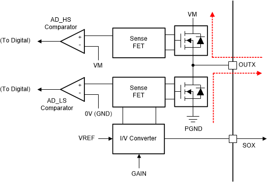
GUID-0EAE14A7-1A6B-4C34-AE60-9BD2C940345F-low.gifFigure 8-31 Active Demagnetization Operation

#GUID-3BC55062-1758-4597-8603-CB06A174FF0E/T5752651-152 shows the configuration of ASR and AAR mode in the DRV8316C-Q1 device.

Table 8-7 OCP/SR Configuration
MODE TypeOCP/SR Pin (DRV8316CT-Q1)SR Bits (DRV8316CR-Q1)OCP SettingASR and AAR Mode
Mode 1Connected to AGNDEN_ASR = 0, EN_AAR = 016 AASR and AAR Disabled
Mode 2Connected to AGND with RMODE1EN_ASR = 0, EN_AAR = 024 AASR and AAR Disabled
Mode 3Hi-ZEN_ASR = 1, EN_AAR = 116 AASR and AAR Enabled
Mode 4Connected to AVDDEN_ASR = 1, EN_AAR = 124 AASR and AAR Enabled