SLES256F May   2010  – May 2022 DRV8312 , DRV8332

PRODUCTION DATA  

  1. Features
  2. Applications
  3. Description
  4. Revision History
  5. Pin Configuration and Functions
  6. Specifications
    1. 6.1 Absolute Maximum Ratings
    2. 6.2 ESD Ratings
    3. 6.3 Recommended Operating Conditions
    4. 6.4 Thermal Information
    5. 6.5 Dissipation Ratings
    6. 6.6 Power Deratings (DRV8312)
    7. 6.7 Electrical Characteristics
    8. 6.8 Typical Characteristics
  7. Detailed Description
    1. 7.1 Overview
    2. 7.2 Functional Block Diagram
    3. 7.3 Feature Description
      1. 7.3.1 Error Reporting
      2. 7.3.2 Device Protection System
        1. 7.3.2.1 Bootstrap Capacitor Undervoltage Protection
          1. 7.3.2.1.1 Overcurrent (OC) Protection
        2. 7.3.2.2 Overtemperature Protection
        3. 7.3.2.3 Undervoltage Protection (UVP) and Power-On Reset (POR)
        4. 7.3.2.4 Device Reset
    4. 7.4 Device Functional Modes
      1. 7.4.1 Different Operational Modes
  8. Application and Implementation
    1. 8.1 Application Information
    2. 8.2 Typical Applications
      1. 8.2.1 Three-Phase Operation
        1. 8.2.1.1 Design Requirements
        2. 8.2.1.2 Detailed Design Procedure
          1. 8.2.1.2.1 Motor Voltage
          2. 8.2.1.2.2 Current Requirement of 12 V Power Supply
          3. 8.2.1.2.3 Voltage of Decoupling Capacitor
          4. 8.2.1.2.4 Overcurrent Threshold
          5. 8.2.1.2.5 Sense Resistor
          6. 8.2.1.2.6 Output Inductor Selection
        3. 8.2.1.3 Application Curves
      2. 8.2.2 DRV8312 Application Diagram for Three-Phase Operation
      3. 8.2.3 Control Signal Logic With Conventional 6 PWM Input Scheme
      4. 8.2.4 Hall Sensor Control With 6 Steps Trapezoidal Scheme
      5. 8.2.5 Sensorless Control With 6 Steps Trapezoidal Scheme
  9. Power Supply Recommendations
    1. 9.1 Bulk Capacitance
    2. 9.2 System Power-Up and Power-Down Sequence
      1. 9.2.1 Powering Up
      2. 9.2.2 Powering Down
    3. 9.3 System Design Recommendations
      1. 9.3.1 VREG Pin
      2. 9.3.2 VDD Pin
      3. 9.3.3 OTW Pin
      4. 9.3.4 FAULT Pin
      5. 9.3.5 OC_ADJ Pin
      6. 9.3.6 PWM_X and RESET_X Pins
      7. 9.3.7 Mode Select Pins
  10. 10Layout
    1. 10.1 Layout Guidelines
      1. 10.1.1 PCB Material Recommendation
      2. 10.1.2 Ground Plane
      3. 10.1.3 Decoupling Capacitor
      4. 10.1.4 AGND
    2. 10.2 Layout Example
      1. 10.2.1 Current Shunt Resistor
        1. 10.2.1.1 66
    3. 10.3 Thermal Considerations
      1. 10.3.1 Thermal Via Design Recommendation
  11. 11Device and Documentation Support
    1. 11.1 Related Links
    2. 11.2 Trademarks
    3. 11.3 Electrostatic Discharge Caution
    4. 11.4 Glossary
  12. 12Mechanical, Packaging, and Orderable Information

Package Options

Mechanical Data (Package|Pins)
Thermal pad, mechanical data (Package|Pins)
Orderable Information

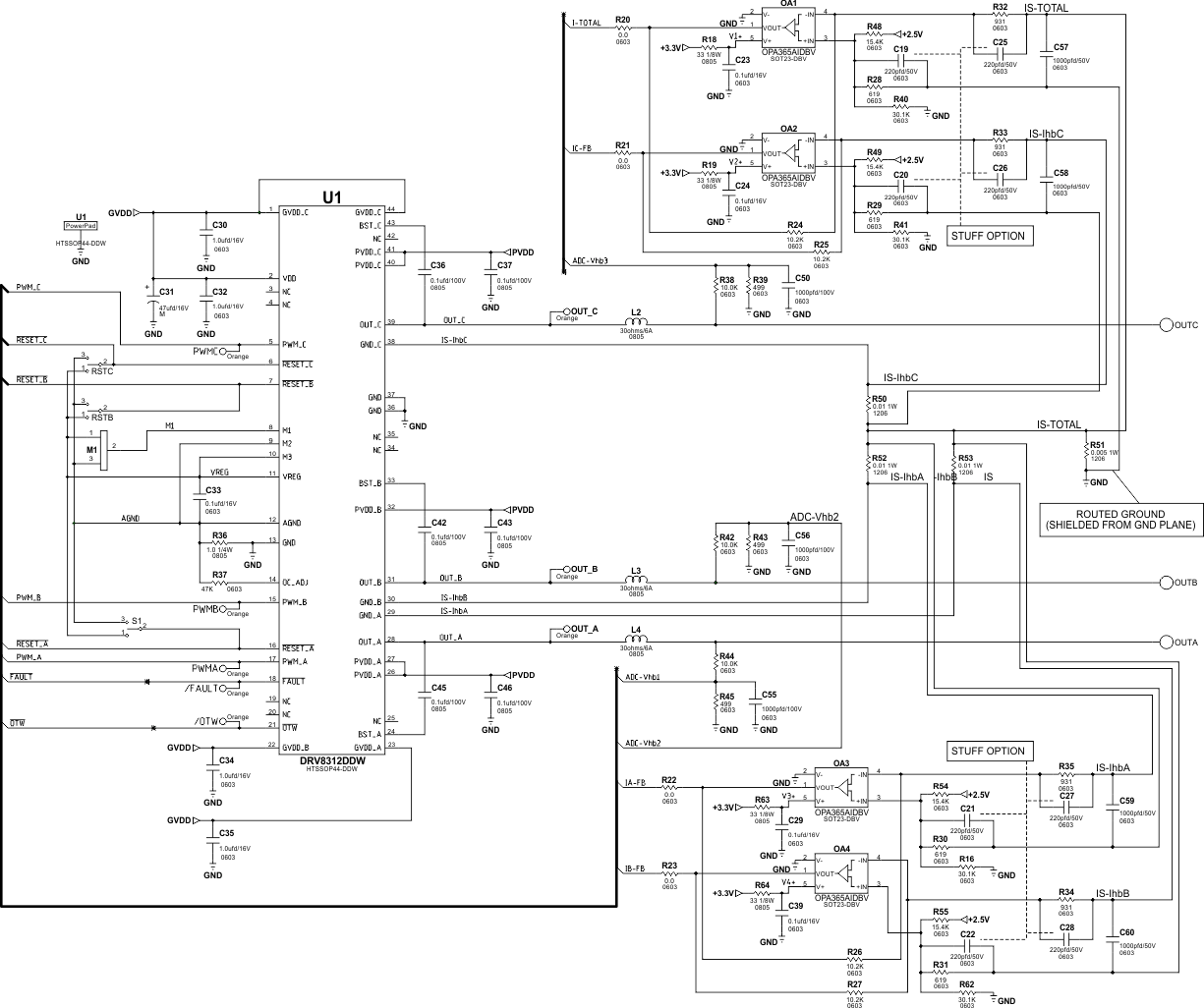
GUID-DFD09B64-1D33-43B3-B715-8EB8576F3B11-low.gifFigure 10-1 DRV8312 Schematic Example
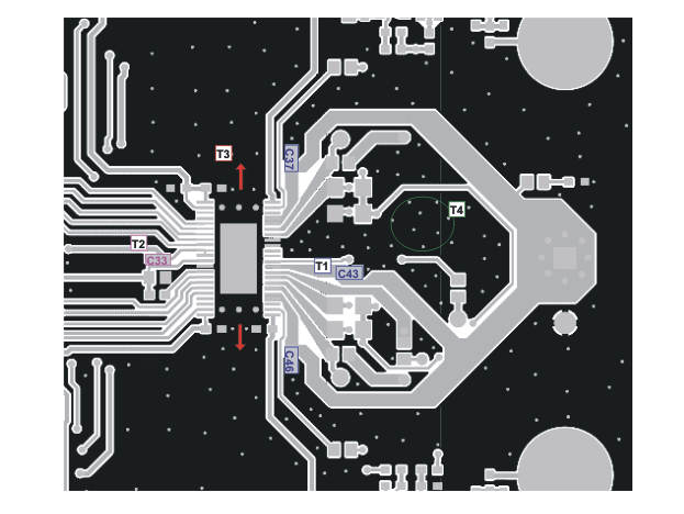
GUID-DE154498-0DF2-4562-A39C-B2F28864D4D7-low.gif
T1: PVDD decoupling capacitors C37, C43, and C46 should be placed very close to PVDD_X pins and ground return path.
T2: VREG decoupling capacitor C33 should be placed very close to VREG abd AGND pins.
T3: Clear the space above and below the device as much as possible to improve the thermal spreading.
T4: Add many vias to reduce the impedance of ground path through top to bottom side. Make traces as wide as possible for ground path such as GND_X path.
Figure 10-2 Printed Circuit Board – Top Layer
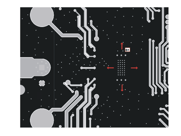
GUID-AE7000C6-4932-48D6-97B2-000397470A69-low.gif
B1: Do not block the heat transfer path at bottom side. Clear as much space as possible for better heat spreading.
Figure 10-3 Printed Circuit Board – Bottom Layer