SLVSHC7 December   2023 DRV8334

PRODUCTION DATA  

  1.   1
  2. Features
  3. Applications
  4. Description
  5. Revision History
  6. Pin Configuration and Functions
    1. 5.1 Pin Functions 48-Pin DRV8334
  7. Specification
    1. 6.1 Absolute Maximum Ratings
    2. 6.2 ESD Ratings DRV8334
    3. 6.3 Recommended Operating Conditions
    4. 6.4 Thermal Information DRV8334
    5. 6.5 Electrical Characteristics
    6. 6.6 Timing Requirements
    7. 6.7 SPI Timing Diagrams
  8. Detailed Description
    1. 7.1 Overview
    2. 7.2 Functional Block Diagram
    3. 7.3 Feature Description
      1. 7.3.1 Three BLDC Gate Drivers
        1. 7.3.1.1 PWM Control Modes
          1. 7.3.1.1.1 6x PWM Mode
          2. 7.3.1.1.2 3x PWM Mode with INLx enable control
          3. 7.3.1.1.3 3x PWM Mode with SPI enable control
          4. 7.3.1.1.4 1x PWM Mode
          5. 7.3.1.1.5 SPI Gate Drive Mode
        2. 7.3.1.2 Gate Drive Architecture
          1. 7.3.1.2.1 Bootstrap diode
          2. 7.3.1.2.2 GVDD Charge pump
          3. 7.3.1.2.3 VCP Trickle Charge pump
          4. 7.3.1.2.4 Gate Driver Output
          5. 7.3.1.2.5 Passive and Semi-active pull-down resistor
          6. 7.3.1.2.6 TDRIVE Gate Drive Timing Control
          7. 7.3.1.2.7 Propagation Delay
          8. 7.3.1.2.8 Deadtime and Cross-Conduction Prevention
      2. 7.3.2 Low-Side Current Sense Amplifiers
        1. 7.3.2.1 Unidirectional Current Sense Operation
        2. 7.3.2.2 Bidirectional Current Sense Operation
      3. 7.3.3 Gate Driver Shutdown
        1. 7.3.3.1 DRVOFF Gate Driver Shutdown
        2. 7.3.3.2 Gate Driver Shutdown Timing Sequence
      4. 7.3.4 Gate Driver Protective Circuits
        1. 7.3.4.1  PVDD Supply Undervoltage Lockout (PVDD_UV)
        2. 7.3.4.2  GVDD Undervoltage Lockout (GVDD_UV)
        3. 7.3.4.3  BST Undervoltage Lockout (BST_UV)
        4. 7.3.4.4  MOSFET VDS Overcurrent Protection (VDS_OCP)
        5. 7.3.4.5  VSENSE Overcurrent Protection (SEN_OCP)
        6. 7.3.4.6  Phase Comparators
        7. 7.3.4.7  Thermal Shutdown (OTSD)
        8. 7.3.4.8  Thermal Warning (OTW)
        9. 7.3.4.9  OTP CRC
        10. 7.3.4.10 SPI Watchdog Timer
    4. 7.4 Device Functional Modes
      1. 7.4.1 Gate Driver Functional Modes
        1. 7.4.1.1 Sleep Mode
        2. 7.4.1.2 Operating Mode
      2. 7.4.2 Device Power Up Sequence
    5. 7.5 Programming
      1. 7.5.1 SPI
      2. 7.5.2 SPI Format
      3. 7.5.3 SPI Format Diagrams
    6. 7.6 Register Maps
      1. 7.6.1 STATUS Registers
      2. 7.6.2 CONTROL Registers
  9. Application and Implementation
    1. 8.1 Application Information
    2. 8.2 Typical Application
      1. 8.2.1 Typical Application with 48-pin package
        1. 8.2.1.1 External Components
      2. 8.2.2 Application Curves
  10. Layout
    1. 9.1 Layout Guidelines
    2. 9.2 Layout Example
  11. 10Device and Documentation Support
    1. 10.1 Documentation Support
      1. 10.1.1 Related Documentation
    2. 10.2 Receiving Notification of Documentation Updates
    3. 10.3 Community Resources
    4. 10.4 Trademarks
  12. 11Mechanical, Packaging, and Orderable Information
    1. 11.1 Package Option Addendum
    2. 11.2 Tape and Reel Information

Package Options

Mechanical Data (Package|Pins)
Thermal pad, mechanical data (Package|Pins)
Orderable Information

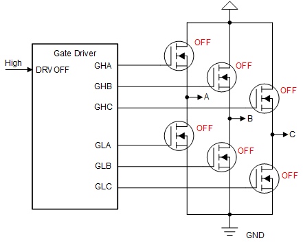
DRVOFF Gate Driver Shutdown

When DRVOFF is driven high, the gate driver goes into shutdown mode, overriding signals on inputs pins INHx and INLx. DRVOFF bypasses the internal digital logic and is connected directly to the predriver. This pin provides a mechanism for externally monitored faults to disable the gate driver directly bypassing the external controller. When the DRVOFF pin is driven high, the device disables the gate driver and triggers the shutdown sequence.
GUID-20210427-CA0I-T7CC-BWBF-V8KDLSPWHX7Q-low.gif Figure 7-14 DRVOFF Gate Driver Output State