SLVSFO2 July 2020 – MONTH DRV8353M
PRODUCTION DATA
- 1 Features
- 2 Applications
- 3 Description
- 4 Revision History
- 5 Device Comparison Table
- 6 Pin Configuration and Functions
- 7 Absolute Maximum Ratings
- 8 ESD Ratings
- 9 Recommended Operating Conditions
- 10Thermal Information
- 11Electrical Characteristics
- 12SPI Timing Requirements
-
13Detailed Description
- 13.1 Overview
- 13.2 Functional Block Diagram
- 13.3
Feature Description
- 13.3.1 Three Phase Smart Gate Drivers
- 13.3.2 DVDD Linear Voltage Regulator
- 13.3.3 Pin Diagrams
- 13.3.4 Low-Side Current-Shunt Amplifiers
- 13.3.5
Gate Driver Protective Circuits
- 13.3.5.1 VM Supply and VDRAIN Undervoltage Lockout (UVLO)
- 13.3.5.2 VCP Charge-Pump and VGLS Regulator Undervoltage Lockout (GDUV)
- 13.3.5.3 MOSFET VDS Overcurrent Protection (VDS_OCP)
- 13.3.5.4 VSENSE Overcurrent Protection (SEN_OCP)
- 13.3.5.5 Gate Driver Fault (GDF)
- 13.3.5.6 Overcurrent Soft Shutdown (OCP Soft)
- 13.3.5.7 Thermal Warning (OTW)
- 13.3.5.8 Thermal Shutdown (OTSD)
- 13.3.5.9 Fault Response Table
- 13.4 Device Functional Modes
- 13.5 Programming
- 13.6
Register Maps
- 13.6.1 Status Registers
- 13.6.2
Control Registers
- 13.6.2.1 Driver Control Register (address = 0x02h)
- 13.6.2.2 Gate Drive HS Register (address = 0x03h)
- 13.6.2.3 Gate Drive LS Register (address = 0x04h)
- 13.6.2.4 OCP Control Register (address = 0x05h)
- 13.6.2.5 CSA Control Register (address = 0x06h)
- 13.6.2.6 Driver Configuration Register (address = 0x07h)
-
14Application and Implementation
- 14.1 Application Information
- 14.2
Typical Application
- 14.2.1
Primary Application
- 14.2.1.1 Design Requirements
- 14.2.1.2 Detailed Design Procedure
- 14.2.1.3 Application Curves
- 14.2.1
Primary Application
- 15Power Supply Recommendations
- 16Layout
- 17Device and Documentation Support
- 18Mechanical, Packaging, and Orderable Information
Package Options
Mechanical Data (Package|Pins)
- RTA|40
Thermal pad, mechanical data (Package|Pins)
- RTA|40
Orderable Information
13.5.1.1.1 SPI Format
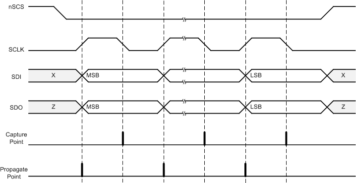
The SDI input data word is 16 bits long and consists of the following format:
- 1 read or write bit, W (bit B15)
- 4 address bits, A (bits B14 through B11)
- 11 data bits, D (bits B11 through B0)
Set the read/write bit (W0, B15) to 0b for a write command. Set the read/write bit (W0, B15) to 1b for a read command.
The SDO output data word is 16 bits long and the first 5 bits are don't care bits. The response word is the data currently in the register being accessed.
Table 13-7 SDI Input Data Word Format
| R/W | ADDRESS | DATA | |||||||||||||
|---|---|---|---|---|---|---|---|---|---|---|---|---|---|---|---|
| B15 | B14 | B13 | B12 | B11 | B10 | B9 | B8 | B7 | B6 | B5 | B4 | B3 | B2 | B1 | B0 |
| W0 | A3 | A2 | A1 | A0 | D10 | D9 | D8 | D7 | D6 | D5 | D4 | D3 | D2 | D1 | D0 |
Table 13-8 SDO Output Data Word Format
| DON'T CARE BITS | DATA | ||||||||||||||
|---|---|---|---|---|---|---|---|---|---|---|---|---|---|---|---|
| B15 | B14 | B13 | B12 | B11 | B10 | B9 | B8 | B7 | B6 | B5 | B4 | B3 | B2 | B1 | B0 |
| X | X | X | X | X | D10 | D9 | D8 | D7 | D6 | D5 | D4 | D3 | D2 | D1 | D0 |
 Figure 13-30 SPI Slave Timing Diagram