SLVSHD4 October   2024 DRV8376

ADVANCE INFORMATION  

  1.   1
  2. Features
  3. Applications
  4. Description
  5. Device Comparison Table
  6. Pin Configuration and Functions
  7. Specifications
    1. 6.1 Absolute Maximum Ratings
    2. 6.2 ESD Ratings
    3. 6.3 Recommended Operating Conditions
    4. 6.4 Thermal Information
    5. 6.5 Electrical Characteristics
    6. 6.6 SPI Timing Requirements
    7. 6.7 SPI Slave Mode Timings
  8. Detailed Description
    1. 7.1 Overview
    2. 7.2 Functional Block Diagram
    3. 7.3 Feature Description
      1. 7.3.1  Output Stage
      2. 7.3.2  Control Modes
        1. 7.3.2.1 6x PWM Mode (PWM_MODE = 00b or 01b or MODE_SR Pin Tied to AGND or in Hi-Z)
        2. 7.3.2.2 3x PWM Mode (xPWM_MODE = 10b or 11b or MODE_SR Pin is Connected to GVDD or to GVDD with RMODE)
      3. 7.3.3  Device Interface Modes
        1. 7.3.3.1 Serial Peripheral Interface (SPI)
        2. 7.3.3.2 Hardware Interface
      4. 7.3.4  AVDD and GVDD Linear Voltage Regulator
      5. 7.3.5  Charge Pump
      6. 7.3.6  Slew Rate Control
      7. 7.3.7  Cross Conduction (Dead Time)
      8. 7.3.8  Propagation Delay
      9. 7.3.9  Pin Diagrams
        1. 7.3.9.1 Logic Level Input Pin (Internal Pulldown)
        2. 7.3.9.2 Logic Level Input Pin (Internal Pullup)
        3. 7.3.9.3 Open Drain Pin
        4. 7.3.9.4 Push Pull Pin
        5. 7.3.9.5 Four Level Input Pin
      10. 7.3.10 Current Sense Amplifiers
        1. 7.3.10.1 Current Sense Amplifier Operation
      11. 7.3.11 Active Demagnetization
        1. 7.3.11.1 Automatic Synchronous Rectification Mode (ASR Mode)
          1. 7.3.11.1.1 Automatic Synchronous Rectification in Commutation
          2. 7.3.11.1.2 Automatic Synchronous Rectification in PWM Mode
        2. 7.3.11.2 Automatic Asynchronous Rectification Mode (AAR Mode)
      12. 7.3.12 Cycle-by-Cycle Current Limit
        1. 7.3.12.1 Cycle by Cycle Current Limit with 100% Duty Cycle Input
      13. 7.3.13 Protections
        1. 7.3.13.1 VM Supply Undervoltage Lockout (RESET)
        2. 7.3.13.2 AVDD Undervoltage Protection (AVDD_UV)
        3. 7.3.13.3 GVDD Undervoltage Lockout (GVDD_UV)
        4. 7.3.13.4 VCP Charge Pump Undervoltage Lockout (CPUV)
        5. 7.3.13.5 Overvoltage Protections (OV)
        6. 7.3.13.6 Overcurrent Protection (OCP)
          1. 7.3.13.6.1 OCP Latched Shutdown (OCP_MODE = 00b)
          2. 7.3.13.6.2 OCP Automatic Retry (OCP_MODE = 01b)
          3. 7.3.13.6.3 OCP Report Only (OCP_MODE = 10b)
          4. 7.3.13.6.4 OCP Disabled (OCP_MODE = 11b)
        7. 7.3.13.7 Thermal Warning (OTW)
        8. 7.3.13.8 Thermal Shutdown (OTS)
    4. 7.4 Device Functional Modes
      1. 7.4.1 Functional Modes
        1. 7.4.1.1 Sleep Mode
        2. 7.4.1.2 Operating Mode
        3. 7.4.1.3 Fault Reset (CLR_FLT or nSLEEP Reset Pulse)
      2. 7.4.2 DRVOFF functionality
    5. 7.5 SPI Communication
      1. 7.5.1 Programming
        1. 7.5.1.1 SPI Format
    6. 7.6 Register Map
      1. 7.6.1 STATUS Registers
      2. 7.6.2 CONTROL Registers
  9. Application and Implementation
    1. 8.1 Application Information
    2. 8.2 Power Supply Recommendations
      1. 8.2.1 Bulk Capacitance
    3. 8.3 Layout
      1. 8.3.1 Layout Guidelines
      2. 8.3.2 Layout Example
      3. 8.3.3 Thermal Considerations
        1. 8.3.3.1 Power Dissipation
  10. Device and Documentation Support
    1. 9.1 Documentation Support
    2. 9.2 Support Resources
    3. 9.3 Trademarks
    4. 9.4 Electrostatic Discharge Caution
    5. 9.5 Glossary
  11. 10Revision History
  12. 11Mechanical, Packaging, and Orderable Information
    1. 11.1 Package Option Addendum
    2. 11.2 Tape and Reel Information

Package Options

Mechanical Data (Package|Pins)
  • NLG|28
Thermal pad, mechanical data (Package|Pins)
Orderable Information

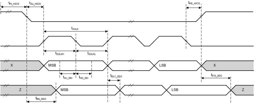
SPI Slave Mode Timings

DRV8376 SPI Secondary Mode TimingsFigure 6-1 SPI Secondary Mode Timings.