SLVSGI0B september 2022 – july 2023 DRV8411
PRODUCTION DATA
- 1
- 1 Features
- 2 Applications
- 3 Description
- 4 Revision History
- 5 Device Comparison
- 6 Pin Configuration and Functions
- 7 Specifications
- 8 Typical Characteristics
- 9 Detailed Description
-
10Application and Implementation
- 10.1 Application Information
- 11Power Supply Recommendations
- 12Layout
- 13Device and Documentation Support
- 14Mechanical, Packaging, and Orderable Information
Package Options
Refer to the PDF data sheet for device specific package drawings
Mechanical Data (Package|Pins)
- PWP|16
- RTE|16
Thermal pad, mechanical data (Package|Pins)
- RTE|16
Orderable Information
9.4.2 Current Regulation
The current through the motor windings may be limited, by the current regulation feature of the DRV8411. For DC motors, current control is used to limit the start-up and stall current of the motor. For stepper motors, current control is often used when the supply rail rating is higher than the motor voltage rating so the winding current remains within the motor specification.
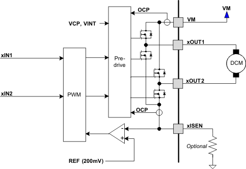
The current regulation feature is implemented with a current chopping scheme. The PWM chopping current, ITRIP, is set by a comparator which compares the voltage across a current sense resistor connected to the xISEN pins with a reference voltage of 200 mV. Figure 9-4 shows the relevant circuitry for current regulation of a single H-bridge in DRV8411.
 Figure 9-4 Current Regulation Circuit
When the motor current reaches the ITRIP level, the device enforces slow current decay by enabling both low-side FETs for a duration of tOFF as shown in Figure 9-5.
 Figure 9-5 Current-Regulation Time Periods
After tOFF elapses, the output is re-enabled according to the two inputs for that bridge, xINx. The device drives current until the motor current reaches the ITRIP level again. The amount of time spent in the drive state depends on the VM voltage, the back-EMF of the motor, and the inductance of the motor. If the state of the INx control pins changes during the tOFF time, the remainder of the tOFF time is ignored, and the outputs will again follow the inputs.
After tOFF elapses, if IOUT is still greater than ITRIP, the H-bridge enters another period of brake/low-side slow decay for tOFF after a drive time of tBLANK..
The chopping current is calculated in Equation 4.
Example: If a 1-Ω sense resistor is used, the chopping current will be 200 mV/1 Ω = 200 mA.
If current regulation is not required, the xISEN pins should be directly connected to the PCB ground plane.