SLES242H December 2009 – July 2024 DRV8412
PRODUCTION DATA
- 1
- 1Features
- 2Applications
- 3Description
- 4Pin Configuration and Functions
- 5Specifications
- 6Detailed Description
-
Application and Implementation
- 7.1 Application Information
- 7.2 Typical Applications
- 7.3 Power Supply Recommendations
- 7.4 Layout
- 7Device and Documentation Support
- 8Revision History
- 9Mechanical, Packaging, and Orderable Information
Package Options
Mechanical Data (Package|Pins)
- DDW|44
Thermal pad, mechanical data (Package|Pins)
- DDW|44
Orderable Information
6.4 Device Functional Modes
The DRV841x2 supports four different modes of operation:
- Dual full bridges (FB) (two PWM inputs each full bridge) or four half bridges (HB) with CBC current limit
- Dual full bridges (two PWM inputs each full bridge) or four half bridges with OC latching shutdown (no CBC current limit)
- Parallel full bridge (PFB) with CBC current limit
- Dual full bridges (one PWM input each full bridge) with CBC current limit
In mode 1 and 2, PWM_A controls half bridge A, PWM_B controls half bridge B, and so forth Figure 7-1 shows an application example for full bridge mode operation.
In parallel full bridge mode (mode 3), PWM_A controls both half bridges A and B, and PWM_B controls both half bridges C and D, while PWM_C and PWM_D pins are not used (recommended to connect to ground). Bridges A and B are synchronized internally (even during CBC), and so are bridges C and D. OUT_A and OUT_B should be connected together and OUT_C and OUT_D should be connected together after the output inductor or ferrite bead. If RESET_AB or RESET_CD are low, all four outputs become high-impedance. Figure 7-8 shows an example of parallel full bridge mode connection.
In mode 4, one PWM signal controls one full bridge to relieve some I/O resource from MCU, that is, PWM_A controls half bridges A and B and PWM_C controls half bridges C and D. In this mode, the operation of half bridge B is complementary to half bridge A, and the operation of half bridge D is complementary to half bridge C. For example, when PWM_A is high, high side FET in half bridge A and low side FET in half bridge B will be on and low side FET in half bridge A and high side FET in half bridge B will be off. Since PWM_B and PWM_D pins are not used in this mode, it is recommended to connect them to ground.
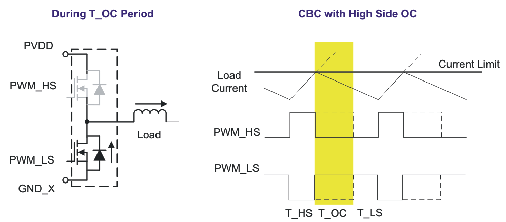
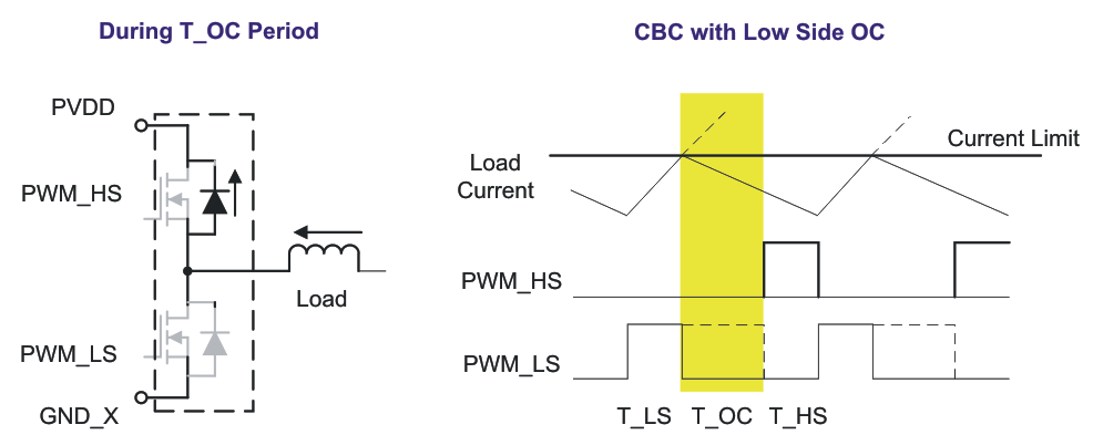
In operation modes 1, 2, and 4 (CBC current limit is used), once the CBC current limit is hit, the driver will be deactivated until the next PWM cycle starts. However, in order for the output to be recovered, the PWM input corresponding to that driver in CBC must be toggled. Because of this, CBC mode does not support operation when one half-bridge PWM input is tied to dc logic level.
Because each half bridge has independent supply and ground pins, a shunt sensing resistor can be inserted between PVDD to PVDD_X or GND_X to GND (ground plane). A high side shunt resistor between PVDD and PVDD_X is recommended for differential current sensing because a high bias voltage on the low side sensing could affect device operation. If low side sensing has to be used, a shunt resistor value of 10 mΩ or less or sense voltage 100mV or less is recommended.

