SLOSE59C May 2020 – July 2022 DRV8424 , DRV8425
PRODUCTION DATA
- 1 Features
- 2 Applications
- 3 Description
- 4 Revision History
- 5 Pin Configuration and Functions
- 6 Specifications
-
7 Detailed Description
- 7.1 Overview
- 7.2 Functional Block Diagram
- 7.3
Feature Description
- 7.3.1 Stepper Motor Driver Current Ratings
- 7.3.2 PWM Motor Drivers
- 7.3.3 Microstepping Indexer
- 7.3.4 Controlling VREF with an MCU DAC
- 7.3.5 Current Regulation
- 7.3.6
Decay Modes
- 7.3.6.1 Slow Decay for Increasing and Decreasing Current
- 7.3.6.2 Slow Decay for Increasing Current, Mixed Decay for Decreasing Current
- 7.3.6.3 Mixed Decay for Increasing and Decreasing Current
- 7.3.6.4 Smart tune Dynamic Decay
- 7.3.6.5 Smart tune Ripple Control
- 7.3.6.6 PWM OFF Time
- 7.3.6.7 Blanking time
- 7.3.7 Charge Pump
- 7.3.8 Linear Voltage Regulators
- 7.3.9 Logic Level, tri-level and quad-level Pin Diagrams
- 7.3.10 nFAULT Pin
- 7.3.11 Protection Circuits
- 7.4 Device Functional Modes
- 8 Application and Implementation
- 9 Power Supply Recommendations
- 10Layout
- 11Device and Documentation Support
- 12Mechanical, Packaging, and Orderable Information
Package Options
Mechanical Data (Package|Pins)
Thermal pad, mechanical data (Package|Pins)
- RGE|24
Orderable Information
5 Pin Configuration and Functions
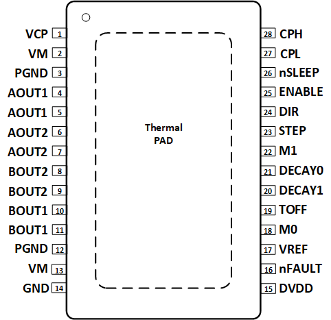
 Figure 5-1 PWP PowerPAD™ Package28-Pin HTSSOPTop View
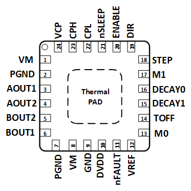
 Figure 5-2 RGE Package24-Pin VQFN with Exposed Thermal PADTop View
Table 5-1 Pin Functions
| PIN | I/O | TYPE | DESCRIPTION | ||
|---|---|---|---|---|---|
| NAME | NO. | ||||
| HTSSOP | VQFN | ||||
| AOUT1 | 4, 5 | 3 | O | Output | Winding A output. Connect to stepper motor winding. |
| AOUT2 | 6, 7 | 4 | O | Output | Winding A output. Connect to stepper motor winding. |
| PGND | 3, 12 | 2, 7 | — | Power | Power ground. Connect to system ground. |
| BOUT2 | 8, 9 | 5 | O | Output | Winding B output. Connect to stepper motor winding |
| BOUT1 | 10, 11 | 6 | O | Output | Winding B output. Connect to stepper motor winding |
| CPH | 28 | 23 | — | Power | Charge pump switching node. Connect a X7R, 0.022-µF, VM-rated ceramic capacitor from CPH to CPL. |
| CPL | 27 | 22 | |||
| DIR | 24 | 19 | I | Input | Direction input. Logic level sets the direction of stepping; internal pulldown resistor. |
| ENABLE | 25 | 20 | I | Input | Logic low to disable device outputs; logic high to enable; internal pullup to DVDD. Also determines the type of OCP and OTSD response. |
| DVDD | 15 | 10 | O | Power | Logic supply voltage. Connect a X7R, 0.47-μF to 1-μF, 6.3-V or 10-V rated ceramic capacitor to GND. |
| GND | 14 | 9 | — | Power | Device ground. Connect to system ground. |
| VREF | 17 | 12 | I | Input | Current set reference input. Maximum value 3.3 V for DRV8424 and 2.64V for DRV8425. DVDD can be used to provide VREF through a resistor divider. |
| M0 | 18 | 13 | I | Input | Microstepping mode-setting pins. Sets the step mode; internal pulldown resistor. |
| M1 | 22 | 17 | |||
| DECAY0 | 21 | 16 | I | Input | Decay-mode setting pins. Sets the decay mode (see the Section 7.3.6 section). |
| DECAY1 | 20 | 15 | |||
| STEP | 23 | 18 | I | Input | Step input. A rising edge causes the indexer to advance one step; internal pulldown resistor. |
| VCP | 1 | 24 | — | Power | Charge pump output. Connect a X7R, 0.22-μF, 16-V ceramic capacitor to VM. |
| VM | 2, 13 | 1, 8 | — | Power | Power supply. Connect to motor supply voltage and bypass to PGND with two 0.01-µF ceramic capacitors (one for each pin) plus a bulk capacitor rated for VM. |
| TOFF | 19 | 14 | I | Input | Sets the Decay mode off time during current chopping; four level pin. Also sets the ripple current in smart tune ripple control mode. |
| nFAULT | 16 | 11 | O | Open Drain | Fault indication. Pulled logic low with fault condition; open-drain output requires an external pullup resistor. |
| nSLEEP | 26 | 21 | I | Input | Sleep mode input. Logic high to enable device; logic low to enter low-power sleep mode; internal pulldown resistor. An nSLEEP low pulse clears faults. |
| PAD | - | - | - | - | Thermal pad. Connect to system ground. |