SLOSE60B May 2020 – May 2022 DRV8424E , DRV8425E
PRODUCTION DATA
- 1 Features
- 2 Applications
- 3 Description
- 4 Revision History
- 5 Pin Configuration and Functions
- 6 Specifications
-
7 Detailed Description
- 7.1 Overview
- 7.2 Functional Block Diagrams
- 7.3 Feature Description
- 7.4 Device Functional Modes
- 8 Application and Implementation
- 9 Power Supply Recommendations
- 10Layout
- 11Device and Documentation Support
- 12Mechanical, Packaging, and Orderable Information
Package Options
Mechanical Data (Package|Pins)
Thermal pad, mechanical data (Package|Pins)
- RGE|24
Orderable Information
5 Pin Configuration and Functions
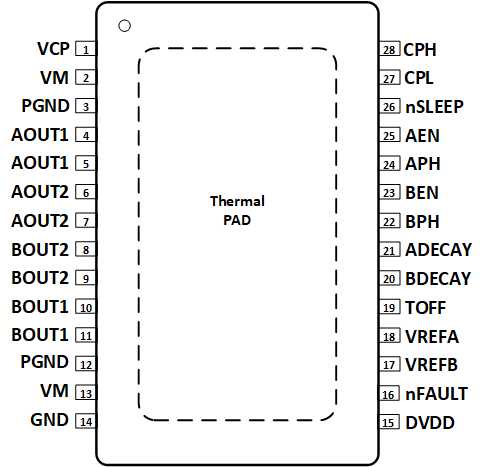
 Figure 5-1 PWP PowerPAD™ Package28-Pin HTSSOPTop View DRV8424E, DRV8425E
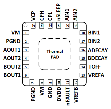
 Figure 5-2 RGE Package24-Pin VQFN with Exposed Thermal PADTop View DRV8424E, DRV8425E
 Figure 5-3 PWP PowerPAD™ Package28-Pin HTSSOPTop View DRV8424P, DRV8425P
 Figure 5-4 RGE Package24-Pin VQFN with Exposed Thermal PADTop View DRV8424P, DRV8425P