SLOSE55C May 2020 – July 2022 DRV8426
PRODUCTION DATA
- 1 Features
- 2 Applications
- 3 Description
- 4 Revision History
- 5 Pin Configuration and Functions
- 6 Specifications
-
7 Detailed Description
- 7.1 Overview
- 7.2 Functional Block Diagram
- 7.3
Feature Description
- 7.3.1 Stepper Motor Driver Current Ratings
- 7.3.2 PWM Motor Drivers
- 7.3.3 Microstepping Indexer
- 7.3.4 Controlling VREF with an MCU DAC
- 7.3.5 Current Regulation
- 7.3.6
Decay Modes
- 7.3.6.1 Slow Decay for Increasing and Decreasing Current
- 7.3.6.2 Slow Decay for Increasing Current, Mixed Decay for Decreasing Current
- 7.3.6.3 Mixed Decay for Increasing and Decreasing Current
- 7.3.6.4 Smart tune Dynamic Decay
- 7.3.6.5 Smart tune Ripple Control
- 7.3.6.6 PWM OFF Time
- 7.3.6.7 Blanking time
- 7.3.7 Charge Pump
- 7.3.8 Linear Voltage Regulators
- 7.3.9 Logic Level, tri-level and quad-level Pin Diagrams
- 7.3.10 nFAULT Pin
- 7.3.11 Protection Circuits
- 7.4 Device Functional Modes
- 8 Application and Implementation
- 9 Power Supply Recommendations
- 10Layout
- 11Device and Documentation Support
- 12Mechanical, Packaging, and Orderable Information
Package Options
Mechanical Data (Package|Pins)
Thermal pad, mechanical data (Package|Pins)
- RGE|24
Orderable Information
7.3.8 Linear Voltage Regulators
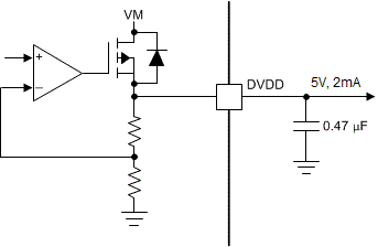
A linear voltage regulator is integrated in the DRV8426 device. The DVDD regulator can be used to provide a reference voltage. DVDD can supply a maximum of 2mA load. For proper operation, bypass the DVDD pin to GND using a ceramic capacitor.
The DVDD output is nominally 5-V. When the DVDD LDO current load exceeds 2mA, the output voltage drops significantly.
 Figure 7-15 Linear Voltage Regulator Block Diagram
If a digital input must be tied permanently high (that is, Mx, DECAYx or TOFF), tying the input to the DVDD pin instead of an external regulator is preferred. This method saves power when the VM pin is not applied or in sleep mode: the DVDD regulator is disabled and current does not flow through the input pulldown resistors. For reference, logic level inputs have a typical pulldown of 200 kΩ.
The nSLEEP pin cannot be tied to DVDD, else the device will never exit sleep mode.